


.
THREE POWER IGBT/MOS AND PULSE
TRANSFORMERDRIVERS
.
CURRENT SENSECOMPARATORWITH 1ms
INHIBITIONTIME FUNCTION
.
INSTANTANEOUS SIGNAL TRANSMISSION
.
0.6 Amp PER CHANNEL PEAK OUTPUT
CURRENT CAPABILITY
.
LOW OUTPUT IMPEDANCETYP :
7Ω at 200mA
.
CMOS/LSTTLCOMPATIBLE INVERTING
INPUTWITH HYSTERESIS
.
4V TO 16V SINGLE SUPPLYOPERATION
.
CURRENT AMPLIFIER
.
LOW BIAS CURRENT TYP: 1.5mA
.
ADJUSTABLE UNDERVOLTAGE
LOCKOUTLEVEL
.
STAND-BY MODE
.
DURING POWER UP NO RANDOM OUTPUT
STATE
.
ENHANCED LATCH-UPIMMUNITY
.
CHANNEL PARALLELINGCAPABILITY
TD310
TRIPLEIGBT/MOS DRIVER
N
DIP16
(Plastic Package)
ORDERCODES
Part Number
TD310I -40
(Plastic Micropackage)
Temperature
Range
o
C, +125oC ••
D
SO16
Package
ND
DESCRIPTION
The TD310 is designedto driveone, two or three
Power IGBT/MOS and has driving capability for
pulse transformer.So itis perfectlysuited to interface control IC with Power Switchesin low side or
half-bridgeconfiguration.
The typicalapplication shown figure 1 implements
the TD310 in a pulse controlled half-bridgedrive.
Positive and negative pulses are applied to the
pulse transformer to charge and discharge the
IGBT/MOS gate capacitance. More sophisticated
secondary circuits provide low impedance gate
drive andshort-circuit protectionas shownin application note n°AN461.
On Figure2, TD310is implementedas a low side
driverin a typical 3 phase motor drive.
Figure 3 presentsa generalpurposelow side gate
drive.
In both case, the current amplifier provides interfacing between a senseresistor and anA/D
converter.
October 1997
PIN CONNECTIONS
+
V
1
CC
IN A
2
3
IN B
4
IN C
Alarm
5
6
7
8
Enable
OA output
OA input +
UVLO/Stdby
16
OUTA
15
14
OUTB
13
OUTC
12
GND
11
Sense -
10
OA input -
9
Sense +
1/9
TD310
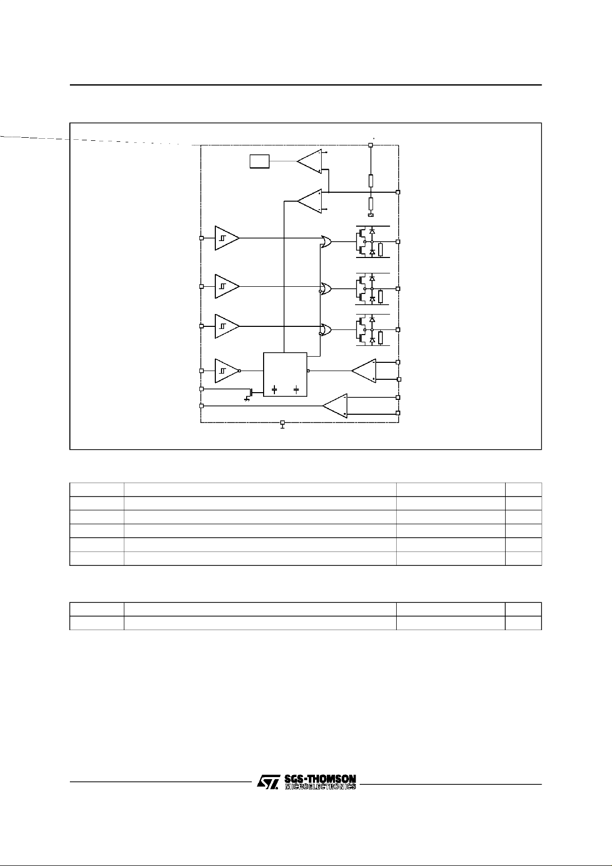
BLOCK DIAGRAM
S tdb y
Stdb y
V
1-
CC
0.7V
2 - Inpu t A
3 - Inpu t B
4 -Input C
5-Enable
6 -Alarm
7 -C urre nt
Output
UVLO
1.2V
Control Un it
tsi tAI
12 - GND
16 - UVLO/Std by
15 - Output A
14 - Output B
13 - Output C
11 - Se nse Input -
9 -S ens e Input +
10 - Current Input -
8 -Cu rrent Input +
ABSOLUTE MAXIMUM RATINGS
Symbol Parameter Value Unit
V
CC
V
V
is
T
T
amb
Supply Voltage 18 V
Input Voltage 0 to V
i
Sense InputVoltage -0.3 to V
Junction Temperature -40 to 150
j
Ambient Temperature -40 to 125
CC
CC
V
V
o
C
o
C
OPERATING CONDITIONS
Symbol Parameter Value Unit
V
CC
Supply Voltage 4 to 16 V
INSTRUCTIONS FORUSE
1 - The TD310 supply voltage must be decoupledwith a 1µF min.capacitor.
2 - If theapplicationinvolving TD310 requires maximum output current capability,
this current must be pulsed : pulse width 1µsec, duty cycle 1% at T
2/9
amb
.
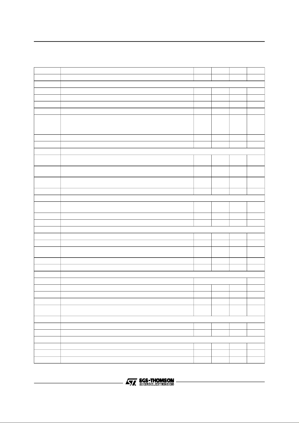
ELECTRICALCHARACTERISTICS
= 15V,T
V
CC
Symbol Parameter Min. Typ. Max. Unit
I
CC
V
IH
V
IL
I
IH
I
IL
t
dH,teH
t
dL,teL
t
ii
t
dd
V
sod
V
sid
V
dem
R
opd
I
s
I
sh
t
A
V
ios
t
Ai
t
s
t
si
V
shys
V
icm
V
io
GBP Gain Bandwidth Product 1 MHz
A
vd
SR Slew Rate at Unity Gain
V
stdby
I
stdby
I
adj
V
st1
V
hys
=25oC (unless otherwisespecified)
amb
Supply Current with Inputs in High State 1.5 2 mA
LOGIC INPUT (all inputs)
High Input Voltage 2 V
Low InputVoltage 0.8 V
High Input Current 10 pA
Low InputCurrent 10 pA
Propagation Delay (10% input to10% output)
Output Rise
Output Fall
≤ T
T
min.
amb
≤ T
200
60
max.
400
400
Input Inhibiting Time 100 ns
Differential Delay Time Between Channels 20 ns
OUTPUT DRIVERS
Sourcing Drop Voltage (A/B/C outputs)
= 200mA 3
I
source
Sinking Drop Voltage (A/B/C outputs)
= 200mA 5
I
sink
Demagnetising Drop Voltage (A/B/C outputs)
= 100mA 2
I
demag.
Output PullDown Resistor 47 kΩ
ALARM OUTPUT
Low LevelSinking Current
= 0.8V 5 35
V
O
High Level SinkingCurrent 1 µA
Alarm Output : Delay Time to Alarm Fall ifSense Input Triggered 500 ns
SENSE INPUT
Input Offset Voltage 20 mV
Inhibition Time ifSense Input Triggered 1 ms
Delay Time to Output Fallif Sense Input Triggered
All outputs inhibited 600
Inhibition Time ofSense Input 300 ns
Sense Hysteresis 40 mV
OPERATIONAL AMPLIFIER
Common Mode Input Voltage Range 0 to V
+
-1.5 V
CC
Input Offset Voltage 10 mV
Open Loop Gain 60 dB
= 100kΩ, CL = 100pF, Vi= 3 to 7V 0.6
R
L
STAND-BY
Standby Mode Threshold Voltage 0.3 1.1 V
Standby Mode Supply Current 30 µA
UNDER VOLTAGE LOCKOUT
Under Voltage Level Adjust Current 1 µA/V
Internal StopThreshold (without external adjustement) 10.7 13.3 V
Threshold Hysteresis 0.8 V
TD310
ns
V
V
V
mA
ns
V/µs
3/9

TD310
UVLO/stbdypin functionning modes
Due to the wide supply voltage range of the TD310, the UVLO function (Under Voltage Lock Out) is
externallyadjustable by a resistorbridge.
The bridge rate can be calculatedin relation with the expectedUVLO protectionlevel as follows:
R1
UVLO
x
R1
V
The internal resistorsets the defaultUVLO value to 12V(*) and might influencethe external bridge rate if
the valuesof the externalresistors are toohigh.
The standbythreshold value depends of the UVLOvalue as follows :
=1.2V(where R1 is the lowerresistor of thebridge)
+R2
stdby
0.7
=
⁄
V
1.2
UVLO
+
via a pull up
CC
V
Both UVLOand stdby functions can be inhibited by connectingthe UVLO/stdby pin to V
resistor (ex 150kΩ).
The following tablesummarizesthe functionsof the TD310:
Pin 16 9/11 5 2/3/4 15/14
Configuration UVLO/stdby Sense+/Sense- EnableIn A/B/C Out
+>- XXLL
Normal 1 H
Stdby 2 L
UVLO 3 M X X X L L OK H
+<-
+>+<- H
HININ
LXL
XXL
/13
A/B/C
6 7/8/10
Alarm Op.
Amp.
OK H (1.5mA)
H
L
HZ L (30µA)
Consumption
Configuration 1 : UVLO/stdby= H
The TD310 is in a normal consumption state (1.5mA), the operationalamplifier is normally functionning
and the buffer outputs are determinedby the sensecomparator inputs, the enableinputs and the buffer
inputs.
Configuration 2 : UVLO/stdby= L
The TD310 isin a lowconsumptionstate (standbymode30µA), the bufferoutputs are set to low state and
the operationalamplifieris inhigh impedance state.
Configuration 3 : UVLO/stdby= M
The V
supply voltage is between V
CC
UVLO
and V
(**). The TD310 remains in a normal consumption
stdby
state and the operationalamplifieris normally functionningbut thebuffer outputsand the alarm pin areset
to lowstate.
(*) If the UVLO level remains unadjusted, it isrecommended to bypass the UVLO/stdby pin with a 1nF capacitor.
(**) If the supply voltage falls below V
4/9
, the TD310 isset in standby mode (configuration 2).
stdby

TIMINGDIAGRAM
TIMING 1
Input
A/B/C
tdH
Output
A/B/C
TIMING 2
Input
A/B/C
TD310
tli
tdL
Output
A/B/C
Sense
Alarm
Enable
Under
Voltage
ts
tAi
tA
tAi
teL
teH
5/9

TD310
TYPICALAPPLICATIONS
Figure1 : THREE PHASEMOTOR DRIVE
15V
1µF
MCU s ignals
ON
Pu lse controlle d inp u ts
TD310
High Volta ge
Pulse transforme r
OFF
Leve lc ontrolled input
enable
interrupt
ADco n ve rter
alarm
CONTROL
UNIT
3 P hase s motor
15V
Rsen s e
6/9

Figure2 : THREE PHASEMOTOR LOW SIDE DRIVE
TD310
Vd
KEYBOARD
DISPLAY
Figure 3 : LOWSIDE DRIVE
ST6
µ
P
+15 V
T1
L6380
B
U
F
F
E
R
1µF
L6380
L6380
T
D
3
1
0
Loa d Load Load
T2
T3
T4 T6
T5
MOTOR
Rsense
7/9

TD310
PACKAGE MECHANICAL DATA
16 PINS - PLASTICDIP
Dimensions
Min. Typ. Max. Min. Typ. Max.
Millimeters Inches
a1 0.51 0.020
B 0.77 1.65 0.030 0.065
b 0.5 0.020
b1 0.25 0.010
D 20 0.787
E 8.5 0.335
e 2.54 0.100
e3 17.78 0.700
F 7.1 0.280
i 5.1 0.201
L 3.3 0.130
Z 1.27 0.050
PM-DIP16.EPS
DIP16.TBL
8/9

PACKAGE MECHANICAL DATA
16 PINS - PLASTICMICROPACKAGE(SO)
TD310
Dimensions
Min. Typ. Max. Min. Typ. Max.
Millimeters Inches
A 1.75 0.069
a1 0.1 0.2 0.004 0.008
a2 1.6 0.063
b 0.35 0.46 0.014 0.018
b1 0.19 0.25 0.007 0.010
C 0.5 0.020
c1 45
o
(typ.)
D 9.8 10 0.386 0.394
E 5.8 6.2 0.228 0.244
e 1.27 0.050
e3 8.89 0.350
F 3.8 4.0 0.150 0.157
G 4.6 5.3 0.181 0.209
L 0.5 1.27 0.020 0.050
M 0.62 0.024
Information furnished is believed to be accurate and reliable. However, SGS-THOMSON Microelectronics assumes no responsibility
for the consequences of use of suchinformation nor forany infringement of patents or other rights of third parties which may result
from its use. No license is granted by implication or otherwise under anypatent or patent rights of SGS-THOMSON Microelectronics.
Specifications mentioned in this publication are subject to change without notice. This publication supersedes and replaces all
information previously supplied. SGS-THOMSON Microelectronics products are not authorized for use as critical components in life
support devices or systems without express written approval of SGS-THOMSON Microelectronics.
PM-SO16.EPS
SO16.TBL
1997 SGS-THOMSON Microelectronics – Printed in Italy – AllRights Reserved
SGS-THOMSON Microelectronics GROUP OF COMPANIES
Australia - Brazil - Canada- China - France - Germany - Hong Kong - Italy - Japan - Korea - Malaysia - Malta - Morocco
The Netherlands - Singapore - Spain - Sweden - Switzerland - Taiwan - Thailand - United Kingdom - U.S.A.
ORDER CODE :
9/9
 Loading...