

ELECTRONIC CIRCUITBREAKER
.TWON-CHANNEL MOSFETs CONTROL AND
DUAL INDEPENDANT CURRENT SUPERVISION FOR OVER CURRENT PROTECTION
.DUALSUPPLYOPERATION
.FROM+3/-5TO+18/-18VOPERATINGVOLT-
AGE
.STEP-UPCONVERTER: V
VOLTAGE
+13.5VOUTPUT
CC
.ADJUSTABLE PROTECTION MODE
(CTRIP1/2)
.INHIBIT FUNCTION
.SHUTDOWNOUTPUT STATUS
.FEWEXTERNAL COMPONENTS
N
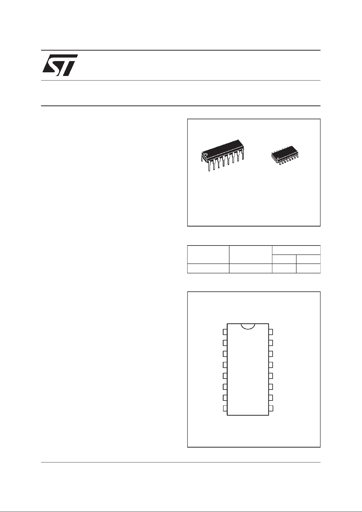
DIP16
(Plastic Package)
ORDERCODES
TD230
D
SO16
(Plastic Micropackage)
DESCRIPTION
The TD230 is designed to control two N-channel
MOSFETsused as powerswitches incircuitbreaking applications.
Its currentsupervisionandimmediateactiononthe
switches ensure high security for the boards and
the suppliesthus protectedagainstshort-circuit or
over current.
Incaseofshort-circuitorovercurrentdetection,the
TD230immediatelyswitchesoffthe corresponding
MOSFET, thus disconnecting the board from the
supply.Afterseveral automaticrestart attempts,a
definitive shutdown of the circuit is done if the
shortcircuit or over current persists over an externally adjustable time, until the TD230 is reset by
temporary INHIBIT signal or temporary switching
off of the power supply (hot disconnection/reconnection).
If the board is disconnectedfromthepositivesupply bytheTD230itwillautomaticallybe disjoncted
from the negativesupply too.
TD230 integrates an induction step-up converter
that provides13.5Vabove the positiverail to drive
the high side MOSFET.
Part Number
TD230I -40
PIN CONNECTIONS
PVcc
LBOOS T
CBOOST
OSC GND
PM1
GND
PM2
NVcc
Temperature
1
2
3
4
5
6
7
8
Package
Range
o
C, +125oC ••
ND
REF1
16
15
GC1
SENSP
14
13
INHIBIT
12
SHUTDOWN
11
SENSN
GC2
10
9
REF2
October 1998
TD230
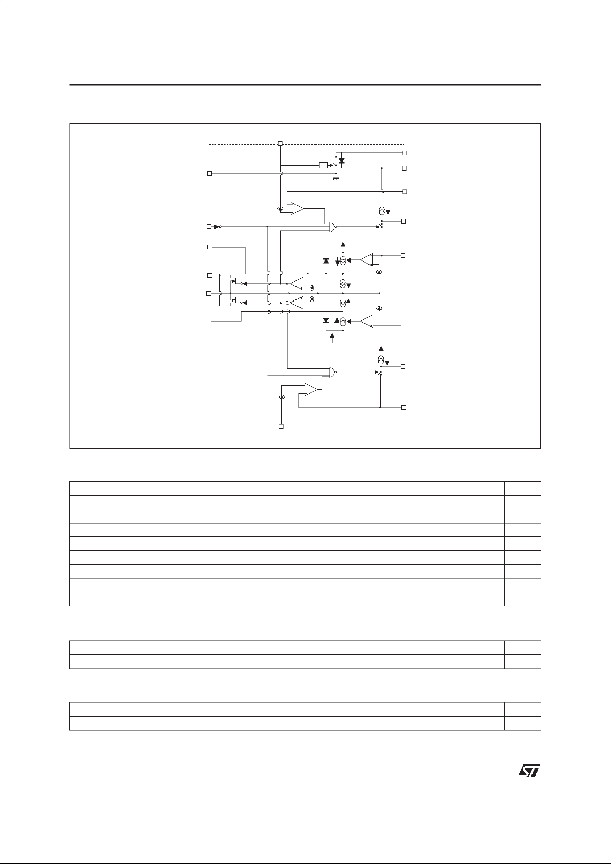
BLOCK DIAGRAM
OS CGND
INHIBIT
S HUTDOWN
GND
PM2
PVcc
STEP-UP
osc
VSP1
PM1
PVcc
IP2
VSP2
VSP3
VSN3
PVcc
IP3
IN3
IN2
VSN2
LBOOST
CBOOS T
REF1
IP1
GC1
SW1
SE NSP
S ENSN
PVcc
IN1
GC2
SW2
VSN1
REF2
NVcc
ABSOLUTE MAXIMUMRATINGS
Symbol Parameter Value Unit
+
V
CC
V
CC
Positive Supply Voltage +22 V
-
Negative Supply Voltage -22 V
Inhibit Input Voltage 7 V
Shutdown Input Voltage 7 V
PM1/PM2 Input Voltage 7 V
T
T
amb
T
stg
Operating Junction Temperature -40to 150
j
Operating Ambient Temperature -40to 125
Storage Temperature Range -65to 150
OPERATINGCONDITIONS
Symbol Parameter Value Unit
V
CC
Supply Voltage +/-18 V
o
C
o
C
o
C
INSTRUCTIONS FOR USE
Symbol Parameter Value Unit
Bypass Capacitor(each supply) 1 µF
2/15
C
bypass

TD230
ELECTRICAL CHARACTERISTICS
= +/-5V, T
V
CC
Symbol Parameter Min. Typ. Max. Unit
SUPPLY
+
V
CC
V
I
CC
Positive Supply Voltage 2.7 18 V
-
Negative Supply Voltage -18 -4.5 V
CC
+
Positive Supply Current
Charge Pump Inactivated 1.8 3 mA
Charge Pump Activated
-
I
CC
Negative Supply Current
Charge Pump Activated/Inactivated
LOGIC INPUT (INHIBIT)
V
V
High Input Voltage 2 6 V
IH
Low Input Voltage 0 0.8 V
IL
tp Propagation Delay GC1/2 (without load) 0.5 2 µs
LOGIC OUTPUT (SHUTDOWN-open drain)
V
I
OH
Low Output Voltage (2mA) 0.8 V
OL
High Output Current (6V) 1 nA
Shutdown Response Time
t
s
(sens P/N shutdown without load) 8 15
STEP-UP CONVERTER
V
boost
t
vboost
V
Step-Up Output Voltage V
Rise Time for V
Output Ripple Voltge 0.15 0.6 V
rip
INPUT COMPARATORS
V
t
Threshold (PVCC- Ref1, NVCC-Ref2) 56 63 71 mV
i
Response Time (GC1/2 - without load) 2 3 µs
re
Inhibition Time (without load) 300 ns
t
i
VOLTAGESOURCES
VSP2
VSN2
VSP3
VSN3
Threshold Sense Pos/Neg 0.7 V
Threshold Protection Mode 1.10 1.20 1.30
CURRENT SOURCES
IP1, IN1 Soft Start Current Sources 10 15 20 µA
IP2, IN2 Protection Mode Current Sources (loading Ctrip 1/2) 3 4 5 µA
IP3, IN3 Protection Mode Current Sources (discharging C
SWITCHES
R
On-Resistance of the switches
on
amb
=25oC, L
=220µH, C
boost
= 100nF (unless otherwise specified)
boost
2.3 4 mA
L
boost
= 220µH, C
boost
= 100nF
-0.7 -1.5 mA
+
+10 V
CC
(10 to 90%) 250 800 µs
boost
CC+/-
) 0.6 1 1.4 µA
trip 1/2
+
CC
0.75 V
+13.4 V
CC+/-
CC
0.8 V
+
SW1/SW2 90 200
+15 V
CC+/-
µs
V
V
Ω
3/15
TD230
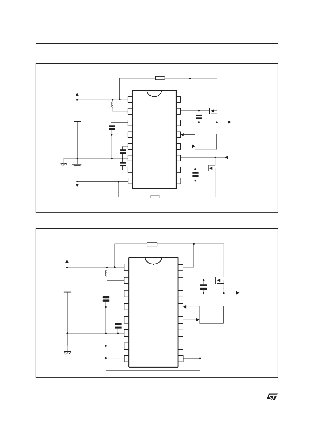
Figure 1 : DUAL ELECTRONIC CIRCUITBREAKER APPLICATION
RS1
Vcc+
REF1
GC1
SENS P
INHIBIT
SHUTDOWN
SE NS N
GC2
REF2
16
15
14
13
12
11
10
9
GND
Vcc-
LBOOST
CBOOST
CTRIP1
CTRIP2
PVcc
1
LBOO ST
2
3
CBOOST
OSCGND
4
PM1
5
GND
6
PM2
7
NVcc
8
CSS1
CONTROL
CSS2
NMos
to BOARD
from BOARD
NMOS
RS2
Figure 2 : SINGLEELECTRONICCIRCUIT BREAKERAPPLICATION
RS1
Vcc+
REF1
GC1
SENSP
INHIBIT
SHUTDOWN
SENSN
GC2
REF2
16
15
14
13
12
11
10
9
GND
LBOOST
CBOOST
CTRIP1
PVcc
1
2
3
LBOOST
CBOOST
OSCGND
4
PM1
5
GND
6
PM2
7
NVcc
8
CSS1
CONTROL
NMos
to BOARD
4/15
TIMING DIAGRAMS
TD230
Events
Sta tus
PVc c-Vre f
(=Vrs)
Vi
SensP
ε
PVcc-
GC1-S ens P
=Vgs
13.4V
~5V
PM1=Vctrip1
PVcc
Vsp3
Norma l
Norma l
Curre nt
Curre nt
Norma l
Norma l
Fun ction
Fun ction
Short Circuit
Short Circuit
Curre nt
Curre nt
Limitation
Limitation
Norma l
Norma l
Curre nt
Curre nt
Norma l
Norma l
Fun ction
Fun ction
Sho rt Circuit
Curre nt
Limitation
Circuit
OFF
Powe r
OFF
ON
Norma l
Curre nt
Norma l
Func tion
ts s # PVc c.Css
Ip1
Inhibit
OFF
HI
LO
Norma l
Current
Norma l
Func tion
S hutdown
PVcc-Vref
(=Vrs)
Vi
GC1 -Se nsP
= Vgs
13.4V
~5V
HiZ
Inhibit
TTL
tpm1 # (Ctrip1.Vsp3)
IP2-IP3
PVcc-Vref
(=Vrs)
Vi
GC1 -Se ns P
= Vgs
13.4V
~5V
ts
tp
t < ti ti tre toff# Ron.Css
5/15

TD230
APPLICATION NOTE
ELECTRONIC CIRCUITBREAKER
by R. LIOU
INTRODUCTION
Over current and short circuit protection is a constant concern for today’s engineers. More and
more applicationsin differentsegments(Telecom,
Automotive,Industrial,Computer...)requirealways
improved reliability after delivery : maintenance
costs are an ever more worrying source of
expensesand customers’dissatisfaction.
Alternatives forshort circuit or over currentprotectionsarethe fusesandthePTC(PositiveTemperature Coefficient)resistors.Thefirst are a cheapbut
destructivesolution; the second are tied to a time
constant due to self heating which is often incompatible with the host equipment’srequirements.
In both cases, a coil can be added foran efficient
limitation of current surges, to the detriment of
weight and volume.
None of these solutions is fully satisfactory for a
reliable, immediate and non destructible short circuit and over current protection.
1. ELECTRONIC CIRCUITBREAKER
The electroniccircuitbreakerTD230istheconvenient solution for any industrial who wants at the
same time :
• immediate, efficientand resettableprotection
for his equipment
• versatility regardingdifferentapplications
• easy and quick design-in
• low componentcount
• low cost
The electroniccircuit breaker TD230 is to be used
with a minimal amount of external and low cost
components to drive one or two N-channel MOSFETs(inrespectivelysingleor dualsupply applications) used as power switches between the DC
power supplies and the equipmentstobe
protected.
The TD230 immediatelyreacts (3µs max. without
load) whenever an over current is detected by
switching off the correspondingMOSFET. Several
automatic restart attempts are made unless the
fault persistsoveranexternallyadjustable amount
of time after which the power MOSFET is definitively switched off, waiting for a reset.
If the fault is detected on the positive supply, the
definitive shutdown will also disconnect the negative power supply and set a warning low level on
the Shutdown pin. If the fault is detected on the
negative supply, the definitive shutdown will disconnectonlythenegativepowersupply,andletthe
positivepart of the circuit undisturbed.
Thewhole system can be reset in three ways :
• byswitching off the power supplies
• by unplugging and re-pluggingthe card(live
insertion)
• by setting the INHIBITpin active during a
short time (allowing remote reset)
2. HOW TO USE THE TD230 ?
The typical configurationoftheTD230 - Electronic
CircuitBreaker- inadual supplytopologyis shown
in figure 1.
In this configuration, both NMOS
are used as
1/2
power switches which connect the equipments to
the powersupplies,thusensuringlowvoltagedrop
through the ON-resistances (Rdson) of NMOS
1/2
2.1. Current Limitation
When an over current condition (I
through the low ohmic shunt resistors R
) is detected
OC
S 1/2
as
given under equation (i) :
• V
RS 1/2=IOCxRS
the gate of the corresponding MOSFET
> 63mV typ. (i)
1/2
is discharged immediately, thus disconnecting the
board/equipmentfromthepower supply.
Note that the over current conditionisgivenby the
constant product I
that the I
OC
OCxRS
limit is directly given by the choice of
the shuntresistors R
= 63mV, which means
values.
S1/2
The TD230 automatically makes restart attempts
by slowly recharging the gate of the MOSFET
1/2
with a 15µAtyp. currentsource ensuringthusslow
ramp with the typical time constant before reconductionshown in equation (ii) :
• t
ON=CISSxVTH
/15µA(ii)
.
6/15

TD230
where C
MOSFET
is the input capacitance of the power
ISS
andVTH, the threshold voltage of the
1/2
MOSFET(typically 5V).
This reconduction time can be extended with an
external soft start capacitor C
figure 1 C
C
ISS+CSS 1/2
will therefore simply be replaced by
ISS
.
SS1/2
as shown in
Figure 1 : Dual ElectronicCircuit Breaker
Application
RS 1
GND
Vcc+
Vcc-
LBOOS T
CBOOST
CTRIP1
CTRIP2
PVcc
1
LBOOS T
2
CBOOS T
3
OSCGND
4
PM1
5
GND
6
PM2
7
NVcc
8
S HUTDOWN
RS2
SE NSP
INHIBIT
S ENSN
REF2
REF1
GC2
16
GC1
15
14
13
12
11
10
9
CSS1
CONTRO L
CSS2
NMos
to BOARD
NMOS
from BOARD
If the fault (over current condition) still remains
afterthereconductionstateoftheMOSFET
been reached, the current through NMOS
1/2
1/2
has
will
overpass the limitation given by equation (i), and
the NMOS
will immediately be switched off
1/2
again.
Figure 2 shows the current limitation which is
operated on every restartattempt.
Figure 2 : TD230as CurrentLimitor
TraceA representstheGate-SourceVoltageofthe
PowerMosfet (0 to 13,4V).
Trace B represents the voltage across the Sense
Resistor (68mΩ) in direct relation with the current
throughit (0 to ~1A).
Note that the firstcurrent peak which is due to an
over current is limited only by the reaction time of
the TD230.
Thisoff time is tied to the value of the external soft
start capacitor C
• t
OFF=RDSONxCSS
While in current limitation mode, the NMOS
by equation(iii) :
SS 1/2
(iii)
1/2
dissipates lowpowerdueto the fact that the ON/OFF
cycle time rate is very low.
Note that the higher the value of C
more the NMOS
will stay in linear mode during
1/2
SS1/2
are, the
currentlimitation.
Note that at Power ON, or in the case of live
insertion,the inrush currentisautomaticallylimited
thanks to the slow gate charge of the MOSFET
whichswitches ON softly due to the time constant
given in equation (ii).
2.2. Fault Time Limitation
The repetitive switching off of the MOSFET will
come to an end under two conditions :
• either the fault has disappeared,and the current through the shuntresistorsR
S 1/2
has
come back to its nominal value : thesystem
keeps runningnormally.
External line defaults (lightning, line breakage,
etc...) are usual causes for such temporary over
currents.
• either the repetitiveswitchingoff has lasted
over an externallyadjustable timeand the
TD230 has definitivelyswitched off the correspondingNMOS: the system waits to bereset.
Equipment faults (component short circuit, over
heat, etc ...) are usual causes for lasting over
currents.
Thisfault time supervisionisdoneby the comparison of the output voltage to 75% of the nominal
supply voltage. As soon as the output voltage is
detected under 0.75xVcc(+/-), the corresponding
external capacitors C
currentsourceI
across C
TRIP1/2
P/N2-IP/N3
reaches 1.20V,the corresponding
TRIP1/2
is charged by a fixed
(3µA). When the voltage
NMOS is definitively switched off and the SHUTDOWN pin is active low.
7/15

TD230
To avoid cumulative charging of the protection
capacitorsC
TRIP 1/2
rent conditions, the capacitors C
in caseof successive overcur-
TRIP 1/2
are con-
Figure3 : FaultTime Limitation
stantlydischargedby anotherfixed currentsource
which valueis a fourth of I
I
P/N3
Trace 1 represents the C
BOOST
(1µA).
P/N2
Voltage (0 to
5+13,4 = 18,4V)
Trace2 representsthe C
The value of the capacitors C
TRIP1
Voltage.
TRIP 1/2
should be
chosenin relationwith therequiredprotectiontime
as indicatedin equation(iv) :
• C
TRIP1/2
where t
=(I
P/N2 - IP/N3
PROTECT 1/2
)xt
PROTECT1/2/VSPN/3
(iv)
is the time defined by the user
before a definitive resettable shutdown of MOS-
1/2
.
FET
Equation (iv) can be translated to :
• C
TRIP 1/2=tPROTECT 1/2
x3µA/ 1.20V (iv)
Note that the positive power supply disjonction
leads to the negative power supply disjonction,
whereas the oppositeisnot true.
2.3. Step-Up Converter
Toensurepropervoltageonthegateof thepositive
supplyNMOS
1(VGS
=13.4V typ), the TD230 integrates a step-up converterwhich is to be boosted
with two small low cost externalcomponents : an
inductorL
anda capacitorC
BOOST
BOOST
, asshown
in figure4.
Figure4 : Step Up Converter External
Components
Rsense
Lboost
Cboost
Sense
Step Up
Driver
TD230
MOS
The principleof this inductive step-up converter is
to pump charges in the tank capacitor C
BOOST
followingthe equation(v) :
Figure5 : Internal Step Up Schematic
Lboost
Cboost
Osc
Regulation
TD230
• V(C
BOOST
)=V
+ 13.4V typ (v)
CC+
Charges are pumped by means of an oscillator
commandedswitch, and storedintheC
BOOST
tank
capacitorthrougha diode as shown on figure 5.
When the voltage across C
+
+13.4V typ, the oscillator is stopped. This
V
CC
BOOST
reaches
createsa ripplevoltagewith an amplitude of0.2V.
Note that the min and max values of V(C
comprised between V
+
+10V and V
CC
CC
BOOST
+
+15V
alreadytakethe ripple voltageintoaccount.
)
8/15

TD230
Properoperation of this step-upconverterisguaranteed at as low as 2.7Vwith a rise time (0 to90%
of V(C
)) in the rangeof 700µs at 2.7V which
BOOST
Figure 6 : Step Up Converter Rise Time
is the worst case. At 5V, the rise time of V(C
is 250µs typ. The C
BOOST
voltage wave form at
boost
power ON under 5V supply voltage is shown on
figure 6.
Trace1 representsthepower supply voltage (0 to
5V).
Trace 2 represents the C
BOOST
Voltageat power
ON (0 to 5+13,4= 18,4V).
Table(a)summerizestherecommendedvaluesof
the C
BOOST
and L
to ensure optimized gate
BOOST
charge and low ripple voltage with their corresponding maximum current surge (I
nal consumption (I
) of the TD230 for the most
CC
) and nomi-
PK
common power supply values. For each power
supplyvalueisalsogiventherecommendedvalue
of a bypass capacitor (C
) on the power sup-
BY
plies.
Note that both C
BOOST
andL
are availablein
BOOST
surface mountpackages.
Table (a) : Recommended values for C
L
+
V
CC
VnFµHmAmVmAµF
2.7 47
5 100 220 35 120 2.5 1
10 100
12 220 470 39 150 2.2 1
14 220 680 34 150 2.4 1
18 220 1000 31 200 2.7 1
boost
C
boostLboostIpk
68 60 190
100
470 33 220
220
V
rip
100
100
I
2.2 1
and
boost
C
cc
by
5>1
2.4. Single SupplyBreakerApplication
The TD230 is perfectly suited to fit in single suppliedapplications(ex 0-5V),andcandriveonlyone
power MOSFET used as high side power switch.
Figure 7 shows how TD230 can be used as a
singlecircuit breaker with thesameperformances.
Figure7 : Single ElectronicCircuit Breaker
Application
RS1
Vcc+
S ENS P
INHIBIT
SHUTDOWN
SE NSN
GC2
REF2
REF1
GC1
16
15
CSS 1
14
13
CO NTROL
12
11
10
9
PVcc
LBOOST
CBOOS T
CTRIP1
)
GND
1
LBOOS T
2
CBOO ST
3
OSCGND
4
PM1
5
GND
6
PM2
7
NVcc
8
In this case, the external componentsconsist in :
one boost inductor, one sense resistor, three ca-
pacitors,and one power MOSFET.
2.5. Typical Telecom Line Cards Protection
Application
One of the typical applications where the TD230
can display all its technical advantages is in an
exchange Telecom Cards protection. Sometimes
fifty cardsor more aretobesuppliedwiththesame
power supply (+/-5V, 1kW), and a decentralized
protection is needed because one card may be
faulty, but should not penalizethe others with unadapted protection system. The risk of complete
breakdownof the system must be eradicated.
In this application the two above described over
current causes (external line perturbationor internalcomponentfault)arelikelytohappen.In thefirst
case,the currentlimitation oneach cardwillensure
undammagingon-boardconditions,andinthesecondcase,the faultycardwill bedisjonctedfromthe
powersupply untilreset.
Figure 8 shows a typical telecom applicationwith
decentralizedprotection.
In thisapplication,thepositivepowersupplyserves
the logic control and analog signals whereas the
negativepower supply is dedicatedto the analog.
NMos
to BOARD
9/15

TD230
Figure 8 : DecentralizedProtection
Vcc+
Power Supply
GND
Vcc-
TD230 TD230 TD230
BOARD1 BOARD2 BOARD3
Therefore,whenafaultappearsonthe positiverail,
the definitive shutdown of the positive NMOS will
lead to the shutdown of the negative NMOS, but
when a fault appears on the negative rail, the
definitiveshutdownofthenegativeNMOSwillhave
no effecton the positiveNMOS.
Severalpossibilitiesare offeredto reset the whole
systemwhen it has beenled to definitive
shutdown :
• the card can be unpluggedandpluggedback
(live insertion)
• the INHIBITpin can be set to active state during a short time (100µs typ or more) in the
case of remote control facilities
3. PERFORMANCES AND EVALUATION
All the curves shown in this application note have
been realizedwith the TD230 EvaluationBoard.
The externalconditionsand components were as
listed hereafter :
• Vcc+ = 5V
• Vcc- = -5V
• Suppliableoutputshort circuitcurrent = 5A
• IC = TD230
• MOSFET
• MOSFET
• L
BOOST
• C
BOOST
= BUZ71
1
= BUZ71
2
=220µH
= 100nF
TD230
BOARDN
• C
•C
•R
• R
• C
• C
TRIP1
TRIP2
= 68mΩ
S1
= 68mΩ
S2
SS1
SS2
=10µF
=10µF
=1nF
=1nF
• PositiveBypass= 4.7µF (plastic)
• Negative Bypass = 4.7µF (plastic)
Theevaluationboardisavailable andallows totest
the performances of the TD230. The layout and
schematic of this evaluation board are given on
figures9A-9B-9C.
4. CAUTIONS
Forproperuse oftheTD230as areliableprotection
device, a fewprecautionsmustbe taken :
1. Properbypasscapacitors mustbeconnectedas
close as possible to the power pinsof the TD230
(PVcc, NVcc, GND). Some recommended values
are givenin table (a).
2. The OSCGND pin must be tied to the GND pin
externally(printedboard)to ensureproperstep-up
converter reference. If not, the step-up converter
will not start.
3. TheINHIBITpin isaCMOS/TTLcompatibleinput
which should therefore not be left unconnected.
Theabsolute maximumrating of this input is 7V. It
should be tied to the TTL compatible output of an
10/15

TD230
Figure9A : PCB(not to scale)
Figure9C : Schematic
Figure9B : Silkscreen
eventual control block, or, if it should not be used,
tied to the GNDpin.
4. The SHUTDOWN pin is an open drain
CMOS/TTLcompatibleoutputwhichshouldbetied
to the TTLcompatibleinput ofan eventualcontrol
block.
The absolute maximum rating of this output is 7V.
In the case ofa visual alarm, a LED is likely to be
tied to the positive power supply which can be
destructive for the Shutdown output if the power
supply is over 7V.An easy way to eliminate this is
to add a 6V zener diode between the Shutdown
output and the Ground as shown on figure 10.
5. Thetime constant ofthe protectionmode (given
by the charge of CTRIP
capacitors) must be
1/2
greater than the time constant of the restart attempts(givenbythechargeoftheCSS
softstart
1/2
capacitors). This condition can be described as
follows :
• V
SP1/2xCTRIP1/2/IP/N2>VTH1/2
(C
SS1/2+CISS1/2
)/I
P/N1
x
11/15

TD230
Figure 10 : VisualAlarm-Shutdown
Vcc+
Shutdown
arerespectively
whereC
TD230
ISS1/2,CSS1/2,VTH1/2,IP/N1
the input capacitance, the soft start capacitor, the
threshold voltage and the internal gate current
sources of NMOS
I
are respectively the voltage source, current
P/N2
; andwhereV
1/2
SP1/2,CTRIP1/2
source and external capacitor of the protection
mode pins PM
V
SP1/2,IP/N2,IP/N1
. Consideringthe typicalvaluesof
1/2
, andthefact that classicalpower
MOSFETshaveathresholdvoltagearound5V,this
condition can be translatedto inequation(vi) :
• C
If C
TRIP1/2
= 1nF and C
ISS
>0.8 x (C
SS1/2+CISS
= 4.7nF, C
SS1/2
)(vi)
TRIP1/2
should
be superior to4.56nF.
Table(b) summerizesProtection Mode Time Con-
stants correspondingto differentC
TRIP1/2
values.
Table (b) : Protection Mode Time Constants
C
TRIP1/2
22nF #10ms
220nF #100ms
2.2µF #1s
22µF #10s
Time Constant Range
for Protection Mode
- Shutdown -
which, in most cases are, are not worrying. But in
someverydemandingapplications,itisnecessary
to remove this noise.
A good way to eliminate such peaks is to add a
resistor connected in series with the inductance
and anelectrolyticcapacitor betweenthecommon
point of resistorandinductance, andgroundofthe
Step-UpConverteras shown on figure 11.
Figure11 : Step Up Noise Reduction
Rse nse
R
C
,
Lboost
TD230
Cboost
The resistor’svoltagedropwillbe due to the product of the average consumption current with the
resistor’svalueandtheinductivecurrentpeakswill
be totally absorbed by the capacitor.Witha 100Ω
resistor, the voltage drop is negligible and the
attenuationgood with a 4.7µF as shown on
figure12.
Figure12 : Step Up Noise Reduction
5. ENHANCEMENTS
The performances of TD230 are well adapted to
most of the circuit breaking applications in many
differents industry segments (Telecom, Automotive, Industrial,Computer etc...),but in the case of
very demanding environment, or outstandingfeatures, the few followingadvices may be helpful.
5.1. Step-Up Noise Reduction
The inductive step-up converter inevitably generates currentpeaksintheoutputofthepowerswitch
12/15

TD230
Trace A represents the ripple voltage on C
BOOST
(200mVwidth).
TraceB representsthevoltageperturbationdueto
the Step-Upconverter on the output (sourceofthe
power Mosfet = Board power supply).
Traces1 and 2 representthesame,but improved
thanks to the Step-UpNoise reductionRC.
5.2. Precision Enhancement
If the system needs accurate current limitation in
an environment subject to very wide temperature
Figure 13 : WideTemperature Variations
Rs ense
R
CTN
R
TD230
variations,a good way to compensatefluctuations
due to temperaturevariations is to use a CTN as
describedin figure 13.
5.3. Temporisation
In some cases,it can be useful to let short current
peakspasswithoutreaction of the breaker,though
theseareofhighervaluethanthefixedcurrentlimit.
This enables the Electronic Circuit Breaker to behave as a thermal disjonctor.
This behaviourcan easily be given by adding an
RC constant as shown on figure 14.
Figure14 : Temporisation
Rsen se
R
C
TD230
13/15

TD230
PACKAGE MECHANICAL DATA
16 PINS - PLASTICDIP
Dimensions
a1 0.51 0.020
B 0.77 1.65 0.030 0.065
b 0.5 0.020
b1 0.25 0.010
D 20 0.787
E 8.5 0.335
e 2.54 0.100
e3 17.78 0.700
F 7.1 0.280
i 5.1 0.201
L 3.3 0.130
Z 1.27 0.050
Min. Typ. Max. Min. Typ. Max.
Millimeters Inches
14/15

PACKAGE MECHANICAL DATA
16 PINS - PLASTICMICROPACKAGE(SO)
TD230
Dimensions
Min. Typ. Max. Min. Typ. Max.
Millimeters Inches
A 1.75 0.069
a1 0.1 0.2 0.004 0.008
a2 1.6 0.063
b 0.35 0.46 0.014 0.018
b1 0.19 0.25 0.007 0.010
C 0.5 0.020
c1 45
o
(typ.)
D 9.8 10 0.386 0.394
E 5.8 6.2 0.228 0.244
e 1.27 0.050
e3 8.89 0.350
F 3.8 4.0 0.150 0.157
G 4.6 5.3 0.181 0.209
L 0.5 1.27 0.020 0.050
M 0.62 0.024
S8
Information furnished is believed to be accurate and reliable. However, STMicroelectronics assumes no responsibility for the
consequences of use of such information nor for any infringementof patents or otherrights of third parties which mayresult from
its use. No license is granted by implication or otherwise under any patent or patent rights of STMicroelectronics. Specifications
mentioned in this publication are subject to change without notice. This publication supersedes and replaces all information
previously supplied.STMicroelectronics productsarenot authorizedfor useas critical components inlife support devices orsystems
without express written approvalof STMicroelectronics.
The STlogo is a trademark of STMicroelectronics
1998 STMicroelectronics – Printed inItaly – All Rights Reserved
STMicroelectronicsGROUP OF COMPANIES
Australia - Brazil - Canada - China - France -Germany - Italy - Japan - Korea- Malaysia - Malta - Mexico- Morocco
The Netherlands - Singapore -Spain - Sweden - Switzerland -Taiwan- Thailand - United Kingdom - U.S.A.
http://www.st.com
o
(max.)
15/15
 Loading...