

A
UA
OA
SOP
C
TC1026
Linear Building Block – Low Power Comparator with
Op Amp and Voltage Reference
Features
• Combines Low-Power OpAmp, Comparator and
Voltage Reference in a Single Package
• Optimized for Single Supply Operation
• SmallPackages:8-PinMSOP,8-PinSOIC,
8-Pin PDI P
• Ultra Low Input Bias Current: Less than 100pA
• Low Quiescent Current: 12µA(Typ.)
• Rail-to-Rail Inputs and Outputs
•OperatesDowntoV
=1.8V,Min
DD
Applications
• Power Management Circuits
• Battery Operated Equipment
• Consumer Products
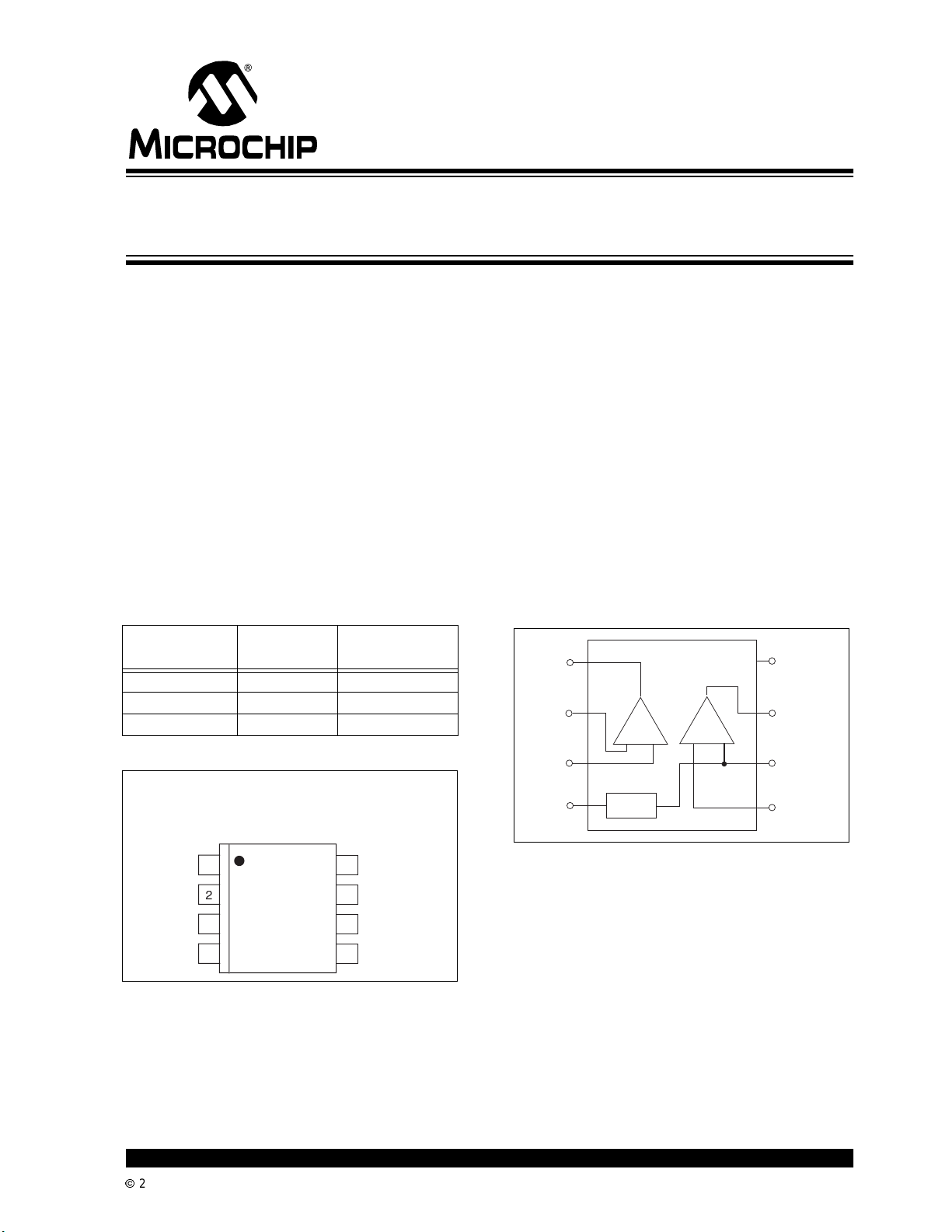
Device Selection Table
Part Number Package
TC1026CEPA 8-Pin PDIP -40°C to +85°C
TC1026CEUA 8-Pin MSOP -40°C to +85°C
TC1026CEOA 8-Pin SOIC -40°C to +85°C
Temperature
Range
Package Types
General Description
The TC1026 is a mixed-function device combining a
general-purpose op amp, comparator and voltage
reference in a single 8-pin package. This increased
integration allows the user to r eplace two or three
packages, which saves space, lowers supply current
and increases system performance.
Both the op amp and comparatorhaverail-to-rail inputs
and outputs which allows operation from low supply
voltages with large input and output swings. The
TC1026 is optimized for low voltage (V
=1.8V),low
DD
supply current (12µA typ) operation.
Packaged in a space-saving 8-Pin MSOP, the TC1026
consumes half the board area of an 8-Pin SOIC and is
ideal for applications requiring high integration, small
size and low power. It is also available i n 8-Pin SOIC
and 8-Pin PDIP packages.
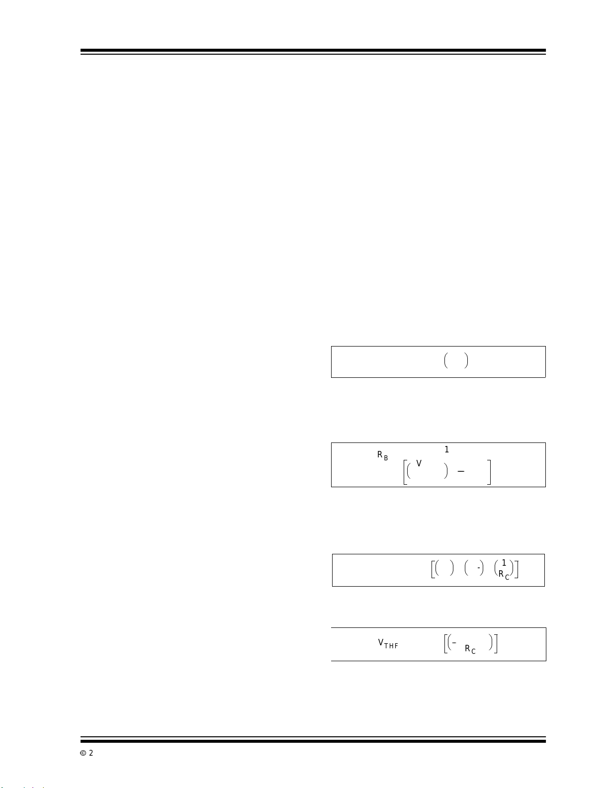
Functional Block Diagram
AMPOUT
AMPIN-
AMPIN+
-
AMP
TC1026
+
+
CMP
1
2
3
8
V
DD
7
CMPOUT
-
6
REF (CMPIN-)
8-Pin PDIP
-Pin M
4
V
SS
Voltage
Reference
5
CMPIN+
-Pin SOI
V
AMPOUT
AMPIN
AMPIN+
V
SS
2002 Microchip TechnologyInc. DS21725B-page 1
TC1026CEP
TC1026CE
TC1026CE
8
DD
CMPOUT
7
REF (CMPIN)
6
CMPIN+
5

TC1026
1.0 ELECTRICAL
CHARACTERISTICS
*Stresses above those listed under "Absolute Maximum
Ratings" may cause permanent damage to the device. These
are stress ratings only and functional operation of the device
at these or any other conditions above those indicated in the
ABSOLUTE MAXIMUM RATINGS*
Supply Voltage......................................................6.0V
operation sections of the specifications is not implied.
Exposure to Absolute Maximum Rating conditions for
extended periods may affectdevice reliability.
Package Power Dissipation:
8-Pin PDIP ...............................................730 mW
8-Pin SOIC...............................................470 mW
8-Pin MSOP .............................................320 mW
Voltage on Any Pin..........(V
– 0.3V) to (VDD+0.3V)
SS
Junction Temperature.......................................+150°C
Operating Temperature Range.............-40°C to +85°C
StorageTemperature Range..............-55°C to +150°C
TC1026 ELECTRICAL SPECIFICATIONS
Electrical Characteristics: Typical values apply at 25°C and VDD=3.0V;TA= -40° to +85°C, and VDD= 1.8V to 5.5V,unless
otherwise specified.
Symbol Parameter Min Typ Max Units Test Conditions
V
DD
I
Q
Op Amp
A
VOL
V
ICMR
V
OS
I
B
V
OS (DRIF T)
GBWP Gain-Bandwidth Product — 90 — kHz V
SR Slew Rate — 35 — mV/µsec CL= 100pF
V
OUT
CMRR Common Mode Rejection Ratio 66 — — dB T
PSRR Power Supply Rejection Ratio 80 — — dB TA=25°C,VCM=V
I
SRC
I
SINK
En Input Noise Voltage — 10 — µVpp 0.1Hz to 10Hz
en Input Noise Voltage Density — 125 — nV/√Hz
Comparator
V
IR
V
OS
I
B
V
OH
V
OL
Supply Voltage 1.8 — 5.5 V
Supply Current — 12 18 µA All outputs unloaded
LargeSignal Voltage Gain — 100 — V/mV RL=10kΩ, VDD=5V
CommonModeInputRange VSS–0.2 — VDD+0.2 V
Input Offset Voltage ±100
±0.3
±500
±1.5
µVmVVDD=3V,VCM=1.5V,TA=25°C
T
= -40°C to 85°C
A
Input Bias Current -100 50 100 pA TA=25°C,VCM=VDDto V
Input Offset Voltage Drift — ±4 — µV/°C VDD=3V,VCM=1.5V
= 1.8V to 5.5V;
DD
V
O=VDD
R
L
Gain = 1
V
IN=VSS
to V
SS
=1MΩ to GND
to V
DD
Output Signal Swing VSS+0.05 — VDD–0.05 V RL=10kΩ
=25°C,VDD=5V
A
V
CM=VDD
VDD=1.8Vto5V
Output Source Current 3 — — mA VIN+=VDD,VIN-=V
OutputShorted to V
VDD=1.8V,Gain=1
OutputSInkCurrent — 125 — nV/Hz IN+ = VSS,IN-=V
OutputShorted to V
VDD=1.8V,Gain=1
to V
SS
SS
SS
SS
DD
DD
1kHz
Input Voltage Range VSS–0.2 — VDD+0.2 V
Input Offset Voltage -5
-5
—
—
+5
+5
mV VDD=3V,TA=25°C
T
= -40°C to 85°C
A
Input Bias Current –– — ±100 pA TA=25°C,IN+=VDDto V
OutputHighVoltage VDD–0.3 — — V RL=10kΩ to V
OutputLowVoltage — — 0.3 V RL=10kΩ to V
SS
DD
SS
SS
DS21725B-page 2
2002 Microchip TechnologyInc.

TC1026
TC1026 ELECTRICAL SPECIFICATIONS (C ONTINUED)
Electrical Characteristics: Typical values apply at 25°C and VDD=3.0V;TA= -40° to +85°C, and VDD= 1.8V to 5.5V,unless
otherwise specified.
Symbol Parameter Min Typ Max Units Test Conditions
PSRR Power Supply Rejection Ratio 60 — — dB T
I
SRC
I
SINK
t
PD1
t
PD2
Output Source Current 1 — — mA IN+ = V
OutputSink Current 2 — — mA IN+ = V
Response Time — 4 — µsec 100mV Overdrive, CL= 100pF
Response Time — 6 — µsec 10mV Overdrive, CL= 100pF
Voltage Reference
V
REF
I
REF(SOURCE)
I
REF(SINK)
C
L(REF)
Reference Voltage 1.176 1.200 1.221 V
Source Current 50 — — µA
Sink Current 50 — — µA
Load Capacitance — — 100 pF
=25°C
A
V
=1.8Vto5V
DD
DD
OutputShortedtoV
VDD=1.8V
SS
OutputShortedtoV
VDD=1.8V
SS
DD
2002 Microchip TechnologyInc. DS21725B-page 3

TC1026
2.0 PIN DESCRIPTION
The description of t he pins are listed in Table 2-1.
TABLE 2-1: PIN FUNCTION TABLE
Pin No.
(8-Pin PDIP)
(8-Pin MSOP)
(8-Pin SOIC)
1 AMPOUT Op amp output.
2 AMPIN- Inverting op amp input.
3 AMPIN+ Non-inverting op amp input.
4V
5 CMPIN+ Non-inverting comparator input.
6 REF(CMPIN) Invertingcomparator input and voltage reference output voltage.
7 CMPOUT Comparator output.
8V
Symbol Description
SS
DD
Negative power supply.
Positive power supply.
DS21725B-page 4
2002 Microchip TechnologyInc.
TC1026
3.0 DETAILED DESCRIPTION
The TC1026 i s one of a series of very low power,linear
building block products targeted at low voltage, single
supply applications. The TC1026 minimum operating
voltageis 1.8V, and typicalsupplycurrentis only 12µA.
It combines a comparator, an op amp and a voltage
reference in a single package.
3.1 Comparator
The TC1026 contains one comparator. The comparator’s input range extends beyond both supply voltages
by 200mV and the outputs will swing to within several
millivolts of the supplies depending on the load current
beingdriven.Theinvertinginputisinternallyconnected
to the output of the reference.
The c omparator exhibitspropagation delay and supply
current which are largely independent of supply
voltage. The low i nput bias current and offset voltage
make it suitable for high impedance precision
applications.
3.2 Operational Amplifier
The TC1026 contains one rail-to-rail op amp. The
amplifier’s i nput range extends beyond both supplies
by 200mV and the outputs will swing to within several
millivolts of the supplies depending on the load current
being driven.
The amplifier design is such that large signal gain, slew
rate and bandwidth are largely independent of supply
voltage.Thelowinput bias current and offsetvoltageof
the TC1026 make it suitable for precisionapplications.
3.3 Voltage Reference
A 2.0% tolerance, internally biased, 1.20V bandgap
voltage reference is included i n the TC1026. It has a
push-pull output capable of sourcing and sinking at
least 50µA.
4.0 TYPICAL APPLICATIONS
The TC1026 lends itself to a wide variety of
applications,particularlyin battery powered systems. It
typically finds application in power management,
processor supervisory and interface circuitry.
4.1 External Hysteresis (Comparator)
Hysteresis can be set externally with three resistors
using positive f eedback techniques (see Figure 4-1).
The design procedure for setting external comparator
hysteresisis as follows:
1. Choose the feedback resistor R
input bias current of the comparator is at most
100pA, the current through R
100nA (i.e., 1000 times the input bias current)
and retain excellent accuracy. The current
through R
R
where VRis a stable reference voltage.
C
at the comparator’s trip point is VR/
C
2. Determinethehysteresis voltage (V
the upper and lower thresholds.
3. Calculate R
as follows:
A
EQUATION 4-1:
V
HY
=
-----------
C
V
DD
RAR
4. Choose the rising threshold voltage for V
(V
).
THR
5. Calculate R
as follows:
B
EQUATION 4-2:
V
THR
1
1
–
-------
R
-----------------------------------------------------------=
R
B
---------------------
VRRA×
6. Verify the t hreshold voltages with these
formulas:
V
rising:
SRC
.Sincethe
C
canbesetto
C
HY
1
–
------R
A
C
)between
SRC
EQUATION 4-3:
V
V
SRC
THR
falling:
VR()RA()
------R
1
A
1
-------
++=
R
B
1
-------
R
C
EQUATION 4-4:
RAVDD×
V
2002 Microchip TechnologyInc. DS21725B-page 5
THF
V
THR
--------- ------------- ---
–=
R
C

TC1026
FIGURE 4-1: CO MPARATOR
EXTERNAL HYSTERESIS
CONFIGURATION
R
C
V
SRC
TC1026
R
A
R
B
V
DD
+
–
TC1026
Comparator
V
R
V
OUT
4.2 Precision Battery Monitor
Figure 4-2 is a precision battery low/battery dead
monitoring circuit. Typically, the battery low output
warns the user that a battery dead condition i s
imminent. Battery dead typically initiates a forced
shutdown to prevent operation at low internal supply
voltages(whichcan cause unstable system operation).
The circuit of Figure 4-2 uses two TC1026 devices and
only six external resistors. AMP 1 is a simple buffer
whileCMPTR1 and CMPTR2 provideprecisionvoltage
detection using V
R4 set the detection threshold for BATT LOW
resistors R1and R3 set the detection threshold for
BATT FAIL
. The component values shown assert
BATT LOW
(typical). Total current consumed by this circuit is
typically 28µA at 3V. Resistors R5 and R6 provide
hysteresis for comparators CMPTR1 and CMPTR2,
respectively.
as a reference. Resistors R2 and
R
while
at 2.2V (typical) and BATT FAIL at 2.0V
4.3 Voice Band Receive Filter
The majority of spectral energy for human voices is in
a 2.7kHz frequency band from 300Hz to 3kHz. To
properly recover a voice signal in applications such as
radios, c ellular phones and voice pagers, a low-power
bandpass filter that is matched to the human voice
spectrum can be implemented using Microchip’s
CMOS op amps. Figure 4-3 shows a unity-gain multipole Butterworth filter with ripple less than 0.15dB in
thehumanvoiceband.Thelower3dBcut-off frequency
is 70Hz (single-orderresponse),whilethe upper cut-off
frequency is 3.5kHz (fourth-order response).
4.4 Supervisory Audio Tone (SAT)
Filter for Cellular
Supervisory Audio Tones (SAT) provide a reliable
transmission path between cellular subscriber units
and base stations. The SAT tone functions much like
the current/voltage used in land l ine telephone systems
to indicate that a phone is off the hook. The SAT tone
may be one of three frequencies: 5970, 6000 or
6030Hz. A loss of SAT implies that channel conditions
are impaired, and if SAT is interrupted for more than 5
seconds, a cellular call is terminated.
Figure 4-4 shows a high Q (30) first order SAT
detection bandpass filter using Microchip’s CMOS op
amp architecture. This circuit nulls all frequencies
except the three SAT tones of interest.
DS21725B-page 6
2002 Microchip TechnologyInc.

FIGURE 4-2: PRECISION BATTERY MONITOR
TC1026
3V
Alkaline
+
V
DD
+
AMP1
–
TC1026
Op Amp
To System DC/DC
Converter
R2, 330k, 1%
R1, 270k, 1%
V
R
R4, 470k, 1%
R5, 7.5M
V
DD
+
CMPTR1
–
Comparator
V
DD
–
CMPTR2
R6, 7.5M
R3, 470k, 1%
Comparator
+
BATTLOW
BATTFAIL
FIGURE 4-3: MULTI-POLE BUTTERWORTH VOICE BAND RECEIVE FILTER
Gain = 0dB
Fch = 3.5kHz
-24dB/Octave
Fcl = 70Hz
+6dB/Octave
Passband Ripple
< 0.15dB
0.1µF
22.6k
6800pF
V
DD
+
–
Op Amp
22.6k
750pF
/2
V
DD
TC1026
V
IN
21.0k 21.0k 21.0k
2400pF
470pF
V
DD
Op Amp
+
–
V
OUT
2002 Microchip TechnologyInc. DS21725B-page 7

TC1026
FIGURE 4-4: SE COND ORDER S AT BANDPASS FILTER
Gain = 0dB
Q = 30
Q = F
C
BW (3dB)
FC = 6kHz
V
IN
TC1026
24.3k
11.2
V
DD
.036µF
/2
48.7k
VDD/2
.036µF
–
+
V
DD
Amp.
V
OUT
DS21725B-page 8
2002 Microchip TechnologyInc.

TC1026
5.0 TYPICAL CHARACTERISTICS
Note: The graphs and tables provided following this note are a statistical summary based on a limited number of
samples and are provided for informational purposes only. The performance characteristics listed herein
are not tested or guaranteed. In some graphs or tables, the data presented may be outside the specified
operating range ( e.g., outside specified power supply range) and therefore outside the warranted range.
Comparator Propagation Delay
vs. Supply Voltage
7
= 25
T
°
C
A
= 100pF
C
L
sec)
µ
6
Overdrive = 10mV
5
4
3.5
4 4.5 5 5.5
3
DELAY TO RISING EDGE (
2
1.5
2
Overdrive = 50mV
2.5 3
SUPPLY VOLTAGE (V) SUPPLY VOLTAGE (V)
Comparator Propagation Delay
vs. Temperature
7
Overdrive = 100mV
sec)
µ
6
V
DD
V
5
4
DELAY TO FALLING EDGE (
3
-40°C85°C25°C
TEMPERATURE (°C)
DD
V
DD
V
DD
= 5V
= 4V
= 3V
= 2V
Comparator Propagation Delay
vs. Supply Voltage
7
= 25
T
°
C
A
= 100pF
C
L
sec)
µ
6
Overdrive = 10mV
5
4
Overdrive = 50mV
3
DELAY TO FALLING EDGE (
2
1.5
2
Overdrive = 100mV
2.5 3
3.5
4 4.5 5 5.5
Comparator Output Swing
vs. Output Source Current
2.5
T
= 25
°
C
A
2.0
(V)
OUT
- V
DD
V
1.5
1.0
V
= 1.8V
DD
.5
0
0
12345 6
I
(mA)
SOURCE
V
V
DD
DD
= 3V
= 5.5V
Comparator Propagation Delay
vs. Temperature
7
Overdrive = 100mV
sec)
µ
6
5
4
DELAY TO RISING EDGE (
3
-40°C85°C25°C
TEMPERATURE (°C)
V
V
V
V
Comparator Output Swing
vs. Output Sink Current
2.5
= 25
T
°
C
A
2.0
(V)
1.5
SS
- V
1.0
OUT
V
.5
0
012 345
I
SINK
V
DD
= 1.8V
V
DD
(mA)
V
= 5.5V
DD
DD
DD
DD
DD
= 5V
= 4V
= 2V
= 3V
= 3V
6
Comparator Output Short-Circuit
Current vs. Supply Voltage
60
50
40
30
20
10
Sourcing
0
OUTPUT SHORT-CIRCUIT CURRENT (mA)
0
2002 Microchip TechnologyInc. DS21725B-page 9
T
Sinking
12345 6
SUPPLY VOLTAGE (V)
= 85°C
A
TA = -40°C
TA = 25°C
= -40
A
T
= 85°C
T
A
T
A
C
°
= 25°C
1.240
1.220
1.200
1.180
1.160
REFERENCE VOLTAGE (V)
1.140
Reference Voltage vs.
Load Current
V
V
= 1.8V
DD
V
= 1.8V
DD
0
24
LOAD CURRENT (mA)
DD
= 3V
V
Sinking
Sourcing
V
V
= 3V
DD
6
DD
DD
8
= 5.5V
= 5.5V
4
3
2
1
0
10
0
SUPPLY AND REFERENCE VOLTAGES (V)
Line Transient
Response of V
V
DD
V
REF
100 200
TIME (µsec)
REF
300
400

TC1026
t
ge
)
(
)
p
e
)
5
0
5
0
5
0
0
000
500
000
025
)
(
)
n
ge
0
0
00
0
0
0
e
e
p
e
)
(
(
)
(
)
00
00
507501000
070
50017502000
00
0
000
5V
t
y
n
t
ge
)
(
)
5
0
5
0
5
30
35
0
C
l
e
)
070
(
)
n
y
)
(
)
0K
00
0
0
30
0
50
60
0
00K
5.0 TYPICAL CHARACTERISTICS (CONTINUED)
Op Amp DC Open-Loop Gai
vs. Supply Volta
14
12
dB
1
4
2
DC OPEN-LOOP GAIN
.01.02.0.04.0.0.
SUPPLY VOLTAGE (V
Op Amp Short-Circuit Curren
vs. Supply Volta
-
mA
-1
-1
-2
-2
UTPUT CURRENT
-
R
Op Amp DC Open-Loop Gain
vs. Tem
2
1
1
-4
TEMPERATURE (C
Op Amp Load Resistanc
vs. Load Capacitanc
1
10% Overshoo
1
k
AD
1
Region of Marginal Stabilit
Region of Stable Operatio
eratur
= 1.
Op Amp Short-Circuit Curren
vs. Supply Volta
4
4
mA
2
2
1
UTPUT CURRENT
1
.01.02.0.04.0.0.
I
SINK
SUPPLY VOLTAGE (V
Op Amp Small-Signal
mV
Transient Res
1
NPUT VOLTAGE
mV
1
ons
.01.02.0.04.0.0.
SUPPLY VOLTAGE (V
Op Amp Large-Signa
mV
NPUT VOLTAGE
DS21725B-page 10
Transient Respons
10204
dB
SRR
TIME (sec
2
12501
Op Amp Power Supply Rejectio
Ratio (PSRR) vs. Frequenc
-1
=
-2
-
-4
-
-
-7
1
FREQUENCY (Hz
1
1
UTPUT VOLTAGE
10204
TIME (sec
2002 Microchip TechnologyInc.

5.0 TYPICAL CHARACTERISTICS (CONTINUED)
TC1026
Reference Voltage
vs. Supply Voltage
1.25
1.20
1.15
1.10
REFERENCE VOLTAGE (V)
1.05
1
23
SUPPLY VOLTAGE (V)
Supply Current vs. Supply Voltage
14
12
A)
µ
(
10
SUPPLY CURRENT
4
5
TA = 85°C
T
= 25°C
= -40°C
T
8
6
4
2
0
A
SUPPLY VOLTAGE (V)
A
645312
2002 Microchip TechnologyInc. DS21725B-page 11

TC1026
6.0 PACKAGING INFORMATION
6.1 Package Marking Information
Package marking data not available at this time.
6.2 Taping Form
Component Taping Orientation for 8-Pin MSOP Devices
PIN 1
User Direction of Feed
W
P
Standard Reel Component Orientation
for TR Suffix Device
Carrier Tape, Number of Components Per Reel and Reel Size
Package Carrier Width (W) Pitch (P) Part Per Full Reel Reel Size
8-Pin MSOP 12 mm 8 mm 2500 13 in
Component Taping Orientation for 8-Pin SOIC (Narrow) Devices
User Direction of Feed
PIN 1
W
DS21725B-page 12
P
Standard Reel Component Orientation
for TR Suffix Device
Carrier Tape, Number of Components Per Reel and Reel Size
Package Carrier Width (W) Pitch (P) Part Per Full Reel Reel Size
8-Pin SOIC (N) 12 mm 8 mm 2500 13 in
2002 Microchip TechnologyInc.

6.3 Package Dimensions
)
)
)
)
)
)
)
)
)
)
)
)
)
)
)
)
)
)
)
)
)
)
)
)
P
-Pin Plastic DI
TC1026
.260 (6.60
.240 (6.10
.045 (1.14
.030 (0.76
.200 (5.08
.140 (3.56
.150 (3.81
.115 (2.92
8-Pin MSOP
.400 (10.16
.348 (8.84
.110 (2.79
.090 (2.29
.022 (0.56
.015 (0.38
PIN 1
.122 (3.10)
.114 (2.90)
.070 (1.78
.040 (1.02
.197 (5.00)
.189 (4.80)
.040 (1.02
.020 (0.51
.310 (7.87
.290 (7.37
.015 (0.38
.008 (0.20
.400 (10.16
.310 (7.87
Dimensions: inches (mm)
.026 (0.65) TYP.
.122 (3.10)
.114 (2.90)
.043 (1.10)
MAX.
.016 (0.40)
.010 (0.25)
2002 Microchip TechnologyInc. DS21725B-page 13
.006 (0.15)
.002 (0.05)
6° MAX.
.028 (0.70)
.016 (0.40)
Dimensions: inches (mm)
.008 (0.20)
.005 (0.13)

TC1026
.
)
)
)
)
)
)
)
)
)
)
)
)
)
)
)
)
C
6.3 Package Dimensions (Continued)
-Pin SOI
.050 (1.27) TYP
.197 (5.00
.189 (4.80
.020 (0.51
.013 (0.33
.157 (3.99
.150 (3.81
.010 (0.25
.004 (0.10
.244 (6.20
.228 (5.79
.069 (1.75
.053 (1.35
.010 (0.25
.007 (0.18
.050 (1.27
.016 (0.40
Dimensions: inches (mm)
DS21725B-page 14
2002 Microchip TechnologyInc.

TC1026
Sales and Support
Data Sheets
Products supportedby a preliminary Data Sheet may have an erratasheet describingminoroperationaldifferences and recommendedworkarounds.To determine if an erratasheetexists for a particulardevice, please contactone of the following:
1. Your local Microchip sales office
2. TheMicrochip Corporate LiteratureCenter U.S. FAX:(480)792-7277
3. The Microchip Worldwide Site (www.microchip.com)
Pleasespecify which device, revision of silicon and Data Sheet (includeLiterature #) you are using.
New Customer Notification System
Register on our web site (www.microchip.com/cn)to receive the most currentinformationon our products.
2002 Microchip Technology Inc. DS21725B-page15

TC1026
NOTES:
DS21725B-page16 2002 Microchip Technology Inc.

TC1026
Information contained in this publication regarding device
applications and the like is intended through suggestion only
and may be superseded by updates. It is your responsibility to
ensure that your application meets with your specifications.
No representation or warranty is given and no liability is
assumed by Microchip Technology Incorporated with respect
to the accuracy or use of such information, or infringementof
patents or other intellectual property rights arising from such
use or otherwise. Use of Microchip’sproductsascriticalcomponents in life support systems is not authorized except with
express written approval by Microchip. No licenses are conveyed, implicitly or otherwise, under any intellectual property
rights.
Trademarks
The Microchip name and logo, the Microchi p logo, FilterLab,
K
EELOQ,microID,MPLAB,PIC,PICmicro,PICMASTER,
PICSTART, PRO MATE, SEEVAL and The Embedded Control
SolutionsCompany areregiste red trademarksof MicrochipTechnologyIncorp or ated in the U.S.A. and other countries .
dsPIC, ECONOMONITOR, FanSense, FlexROM, fuzzyLAB,
In-Circuit Serial Programming, ICSP, ICEPIC, microPort,
Migratable Memory, MPASM, MPLIB, MPLINK, MPSIM,
MXDEV, PICC, PICDEM, PICDEM.net , rfPIC, Select Mode
and Total Enduranceare trademarksof MicrochipTechnology
Incorporated in the U.S.A.
Serialized Quick Turn Programming (SQTP) is a service mark
of Microchip Technology Incorporated in the U.S.A.
All other trademarks mentioned herein are property of their
respective companies.
© 2002, Microchip Technology Incorporated, Printed in the
U.S.A., All Rights Reserved.
Printed on recycled paper.
Microchip received QS-9000 quality system
certification for its worldwide headquarters,
design and wafer fabrication facilities in
Chandler and Tempe, Arizona in July 1999
and Mountain View, California in March 2002.
The Company’s quality system processes and
procedures are QS-9000 compliant for its
®
PICmicro
devices, Serial EEPROMs, microperipherals,
non-volatile memory and analog products. In
addition, Microchip’s quality system for the
design and manufacture of development
systemsisISO 9001certified.
2002 Microchip TechnologyInc. DS21725B-page 17
8-bit MCUs, KEELOQ®code hopping

WORLDWIDE SALES AND SERVICE
AMERICAS
Corporate Office
2355 West Chandler Blvd.
Chandler, AZ 85224-6199
Tel: 480-792-7200 Fax: 480-792-7277
Technical Support: 480-792-7627
Web Address: http://www.microchip.com
Rocky Mountain
2355 West Chandler Blvd.
Chandler, AZ 85224-6199
Tel: 480-792-7966 Fax: 480-792-7456
Atlanta
500 Sugar Mill Road, Suite 200B
Atlanta, GA 30350
Tel: 770-640-0034 Fax: 770-640-0307
Boston
2 Lan Drive, Suite 120
Westford, MA 01886
Tel: 978-692-3848 Fax: 978-692-3821
Chicago
333 Pierce Road, Suite 180
Itasca, IL 60143
Tel: 630-285-0071 Fax: 630-285-0075
Dallas
4570 Westgrove Drive, Suite 160
Addison, TX 75001
Tel: 972-818-7423 Fax: 972-818-2924
Detroit
Tri-Atria Office Building
32255 Northwestern Highway, Suite 190
Farmington Hills, MI 48334
Tel: 248-538-2250 Fax: 248-538-2260
Kokomo
2767 S. Albright Road
Kokomo, Indiana 46902
Tel: 765-864-8360 Fax: 765-864-8387
Los Angeles
18201 Von Karman, Suite 1090
Irvine, CA 92612
Tel: 949-263-1888 Fax: 949-263-1338
New York
150 Motor Parkway, Suite 202
Hauppauge, NY 11788
Tel: 631-273-5305 Fax: 631-273-5335
San Jose
Microchip Technology Inc.
2107 North First Street, Suite 590
San Jose, CA 95131
Tel: 408-436-7950 Fax: 408-436-7955
Toro nto
6285 Northam Drive, Suite 108
Mississauga, Ontario L4V 1X5, Canada
Tel: 905-673-0699 Fax: 905-673-6509
ASIA/PACIFIC
Australia
Microchip Technology Australia Pty Ltd
Suite 22, 41 Rawson Street
Epping 2121, NSW
Australia
Tel: 61-2-9868-6733 Fax: 61-2-9868-6755
China - Beijing
Microchip Technology Consulting (Shanghai)
Co., Ltd., Beijing Liaison Office
Unit 915
Bei Hai Wan Tai Bldg.
No. 6 Chaoyangmen Beidajie
Beijing, 100027, No. China
Tel: 86-10-85282100 Fax: 86-10-85282104
China - Chengdu
Microchip Technology Consulting (Shanghai)
Co., Ltd., Chengdu Liaison Office
Rm. 2401, 24th Floor,
Ming Xing Financial Tower
No. 88 TIDU Street
Chengdu 610016, China
Tel: 86-28-6766200 Fax: 86-28-6766599
China - Fuzhou
Microchip Technology Consulting (Shanghai)
Co., Ltd., Fuzhou Liaison Office
Unit 28F, World Trade Plaza
No. 71 Wusi Road
Fuzhou 350001, China
Tel: 86-591-7503506 Fax: 86-591-7503521
China - Shanghai
Microchip Technology Consulting (Shanghai)
Co., Ltd.
Room 701, Bldg. B
Far East International Plaza
No. 317 Xian Xia Road
Shanghai, 200051
Tel: 86-21-6275-5700 Fax: 86-21-6275-5060
China - Shenzh en
Microchip Technology Consulting (Shanghai)
Co., Ltd., Shenzhen Liaison Office
Rm. 1315, 13/F , Shenzhen Kerry Centre,
Renminnan Lu
Shenzhen 518001, China
Tel: 86-755-2350361 Fax: 86-755-2366086
Hong Kong
Microchip Technology Hongkong Ltd.
Unit 901-6, Tower2, Metroplaza
223 Hing Fong Road
Kwai Fong, N.T., Hong Kong
Tel: 852-2401-1200 Fax: 852-2401-3431
India
Microchip Technology Inc.
India Liaison Office
Divyasree Chambers
1 Floor, Wing A (A3/A4)
No. 11, O’Shaugnessey Road
Bangalore, 560 025, India
Tel: 91-80-2290061 Fax: 91-80-2290062
Japan
Microchip Technology Japan K.K.
Benex S-1 6F
3-18-20, Shinyokohama
Kohoku-Ku, Yokohama-shi
Kanagawa, 222-0033, Japan
Tel: 81-45-471- 6166 Fax: 81-45-471-6122
Korea
Microchip Technology Korea
168-1, Youngbo Bldg. 3 Floor
Samsung-Dong, Kangnam-Ku
Seoul, Korea 135-882
Tel: 82-2-554-7200 Fax: 82-2-558-5934
Singapore
Microchip Technology Singapore Pte Ltd.
200 Middle Road
#07-02 Prime Centre
Singapore, 188980
Tel: 65-6334-8870 Fax: 65-6334-8850
Ta iw an
Microchip Technology Taiwan
11F-3, No. 207
Tung Hua North Road
Taipei, 105, Taiwan
Tel: 886-2-2717-7175 Fax: 886-2-2545-0139
EUROPE
Denmark
Microchip Technology Nordic ApS
Regus Business Centre
Lautrup hoj 1-3
Ballerup DK-2750 Denmark
Tel: 45 4420 9895 Fax: 45 4420 9910
France
Microchip Technology SARL
Parc d’Activite du Moulin de Massy
43 Rue du Saule Trapu
Batiment A - ler Etage
91300 Massy, France
Tel: 33-1-69-53-63-20 Fax: 33-1-69-30-90-79
Germany
Microchip Technology GmbH
Gustav-Heinemann Ring 125
D-81739 Munich, Germany
Tel: 49-89-627-144 0 Fax: 49-89-627-144-44
Italy
Microchip Technology SRL
Centro Direzionale Colleoni
Palazzo Taurus 1 V. Le Colleoni 1
20041 Agrate Brianza
Milan, Italy
Tel: 39-039-65791-1 Fax: 39-039-6899883
United Kingdom
Arizona Microchip Technology Ltd.
505 Eskdale Road
Winnersh Triangle
Wokingham
Berkshire,England RG415TU
Tel: 44 118 921 5869 Fax: 44-118 921-5820
03/01/02
DS21725B-page 18
*DS21725B*
2002 Microchip Technology Inc.
 Loading...