

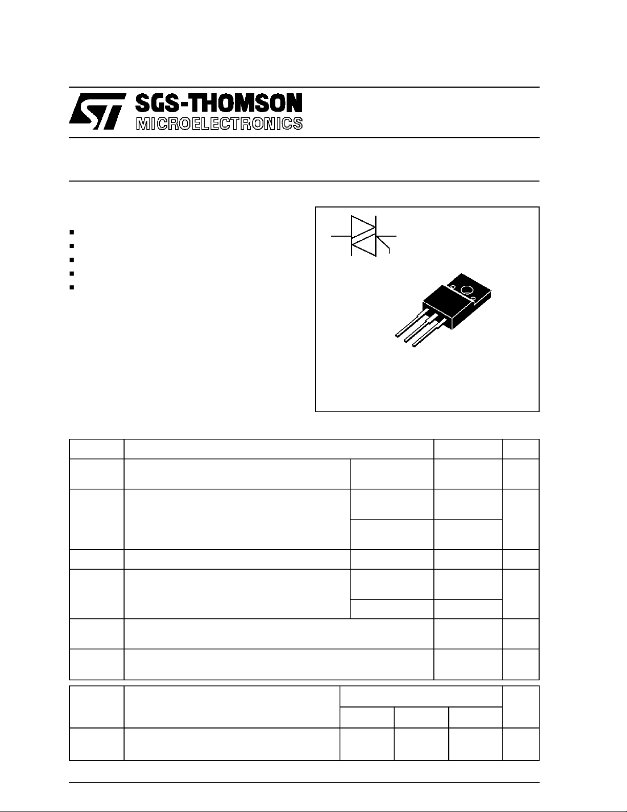
T620W
FEATURES
=6A
I
TRMS
V
DRM=VRRM
=400V to 700V
EXCELLENTSWITCHINGPERFORMANCES
INSULATINGVOLTAGE= 1500V
(RMS)
U.L. RECOGNIZED: E81734
DESCRIPTION
TheT620/630Wtriacs usehighperformanceglass
passivated chip technology, housed in a fully
moldedplasticISOWATT220ABpackage.
TM
The SNUBBERLESS
concept offers suppression of R-C network, and is suitable for applications such as phase control and static switch on
inductiveand resistive loads.
T630W
SNUBBERLESS TRIAC
A
2
A
1
G
A
1
A
2
G
ISOWATT220AB
(Plastic)
ABSOLUTERATINGS (limiting values)
Symbol Parameter Value Unit
I
T(RMS)
RMS on-statecurrent
Tc=100°C6A
(360° conductionangle)
I
TSM
Non repetitivesurgepeak on-state current
(T
initial= 25°C)
j
tp = 16.7 ms
(1 cycle, 60 Hz)
tp =10 ms
66 A
75
(1/2 cycle, 50 Hz)
2
tI
I
dI/dt Criticalrateof rise of on-state current
2
t Value(half-cycle,50 Hz) tp =10 ms 28 A2s
Gate supply: I
=500mA dIG/dt =1A/µs.
G
Repetitive
F = 50Hz
20 A/µs
NonRepetitive 100
T
stg
T
j
Storagetemperaturerange
Operatingjunctiontemperature range
Tl Maximumlead temperaturefor soldering during 10s at4.5 mm
- 40to +150
- 40to +125
260 °C
from case
Symbol Parameter
T620/ 630-xxxW
400 600 700
°C
Unit
V
DRM
V
RRM
April 1995
Repetitivepeak off-statevoltage
T
=125°C
j
400 600 700 V
1/5
T620W / 630W
THERMAL RESISTANCES
Symbol Parameter Value Unit
Rth(j-a) Junctionto ambient 50 °C/W
Rth(j-c) Junction to casefor A.C (360°conductionangle) 3.4 °C/W
GATE CHARACTERISTICS (maximumvalues)
P
=1W PGM=10 W(tp =20 µs) IGM=4A(tp=20µs)
G (AV)
ELECTRICALCHARACTERISTICS
Symbol TestConditions Quadrant T620 T630 Unit
I
GT
V
GT
V
GD
tgt V
I
*I
H
V
TM
I
DRM
I
RRM
VD=12V (DC) RL=33Ω
Tj= 25°C I-II-III MAX 20 30 mA
VD=12V (DC) RL=33Ω Tj= 25°C I-II-III MAX 1.5 V
VD=V
DRMRL
D=VDRMIG
/dt= 3Aµs
dl
G
= 100mA Gate open Tj= 25°C MAX 35 50
T
=3.3kΩ Tj= 125°C I-II-III MIN 0.2 V
=500mA
Tj= 25°C I-II-III TYP 2 µs
*ITM= 8.5A tp= 380µs Tj=25°C MAX 1.5 V
VDRMrated
V
rated
RRM
Tj= 25°C MAX 10 µA
Tj= 125°C MAX 2 mA
dV/dt* Linearslopeup to
=67%V
V
D
DRM
Gate open
Tj= 125°C MIN 200 300 V/µs
(dV/dt)c* (dI/dt)c= 3.3 A/ms (seenote) Tj= 125°C MIN 10 20 V/µs
* For either polarity of electrode A2voltage with referenceto electrode A1.
Note : Inusual applications where (dI/dt)c is below 3.3 A/ms,the (dV/dt)c isalways lowerthan10V/µs, and, therefore, it is unnecessary touse
a snuber R-C network accross T620W / T630W triacs.
2/5

T620W / 630W
Fig.1 : Maximum power dissipation versus RMS
on-state current.
P(W)
8
6
4
=30
O
180
=60
o
=90
o
= 120
o
=180
o
o
2
I (A)
0
0123456
T(RMS)
Fig.3: RMSon-state currentversuscasetempera-
ture.
I (A)
T(RMS)
7
6
o
5
4
3
2
= 180
Fig.2: Correlationbetweenmaximumpower dissipation and maximum allowable temperature
(TambandTcase)fordifferentthermal resistances
heatsink+contact.
o
P(W)
Tcase ( C)
8-95
-100
6
Rth = 0 C/W
4
o
o
2.5 C/W
o
5 C/W
o
10 C/W
-105
-110
-115
2
o
Tamb ( C)
0
0 102030405060708090100110120130
-120
-125
Fig.4 : Thermal transient impedance junction to
case and junction to ambient versus pulse duration.
Zth/Rth
1
Zth(j-c)
0.1
Zth( j-a )
0.01
1
0
0 102030405060708090100110120130
o
Tcase( C)
Fig.5: Relativevariationof gatetriggercurrentand
holding current versus junction temperature.
Igt[Tj]
Igt[Tj=25 C]
2.6
2.4
2.2
2.0
1.8
1.6
1.4
Ih
1.2
1.0
0.8
0.6
0.4
-40 -20 0 20 40 60 80 100 120 140
o
Igt
Tj( C)
Ih[Tj]
Ih[Tj=25 C]
o
o
tp(s )
1E-3
1E-2 1E-1 1E+0
1E+1
1E+2 5E+2
Fig.6 : Non repetitive surge peak on-state current
versusnumber ofcycles.
I (A)
TSM
70
60
50
40
30
20
10
Number of cycles
0
1101001000
Tj initial = 25 C
o
3/5

T620W / 630W
Fig.7 : Non repetitivesurge peakon-statecurrent
for a sinusoidalpulse with width : tp ≤ 10ms,and
correspondingvalue ofI
I (A). I2t(A2s)
TSM
1000
100
10
2
t.
I
TSM
I2t
o
Tj initial = 2 5 C
Fig.8: On-statecharacteristics(maximumvalues).
I (A)
TM
100
Tj initial
o
25 C
10
Tj max
1
tp(ms)
1
110
0.1
00.511.522.533.544.555.5
Tj max
Vto =0.9V
Rt =0.062
V (V)
TM
4/5

PACKAGEMECHANICAL DATA
ISOWATT220AB
T620W / 630W
DIMENSIONS
REF.
A 10 10.4 0.393 0.409
B 15.9 16.4 0.626 0.645
B1 9.8 10.6 0.385 0.417
C 28.6 30.6 1.126 1.204
D 16 typ 0.630 typ
E 9 9.3 0.354 0.366
H 4.4 4.6 0.173 0.181
I 3 3.2 0.118 0.126
J 2.5 2.7 0.098 0.106
L 0.4 0.7 0.015 0.027
M 2.5 2.75 0.098 0.108
N 4.95 5.2 0.195 0.204
N1 2.4 2.7 0.094 0.106
O 1.15 1.7 0.045 0.067
P 0.75 1 0.030 0.039
Millimeters Inches
Min. Max. Min. Max.
Cooling method : C
Marking: Typenumber
Weight: 2.1g
Recommendedtorquevalue: 0.55m.N.
Maximum torque value : 0.70 m.N.
Information furnished is believed to be accurate and reliable. However, SGS-THOMSON Microelectronics assumes no responsability for the
consequences ofuse of such information nor for any infringement of patentsor other rights ofthird parties which may result from its use. No
license is granted by implication or otherwise under any patent or patent rights of SGS-THOMSON Microelectronics.Specifications mentioned
in this publication are subject to change without notice. This publication supersedes and replaces all information previously supplied.
SGS-THOMSONMicroelectronics productsare not authorized foruse as critical componentsin life supportdevices or systemswithout express
written approval of SGS-THOMSON Microelectronics.
1995 SGS-THOMSON Microelectronics -Printedin Italy - All rightsreserved.
SGS-THOMSON Microelectronics GROUP OF COMPANIES
Australia - Brazil - France - Germany - Hong Kong - Italy - Japan - Korea - Malaysia- Malta - Morocco - The Netherlands -
Singapore -Spain- Sweden - Switzerland - Taiwan - Thailand - United Kingdom - U.S.A.
5/5
 Loading...