

SGS Thomson Microelectronics T435-800W, T435-800H, T435-800T, T435-700W, T435-700T Datasheet
...
®
T4 Series
SNUBBERLESS™ & LOGIC LEVEL 4A TRIACS
MAIN FEATURES:
Symbol Value Unit
I
T(RMS)
V
DRM/VRRM
I
GTT (Q1)
4A
600 to 800 V
5 to 35 mA
DESCRIPTION
Based on ST’s Snubberless / Logic level technology providing h igh comm ut ation perfo rmances , t he
T4 series is suitable for use on AC inductive loads.
They are recommended for applications using
universal motors, electrovalves.... such as kitchen
aid equipments, power tools, dishwashers,...
Available in a fully insulated package, the
T4...-...W version complies with UL standards (ref.
E81734).
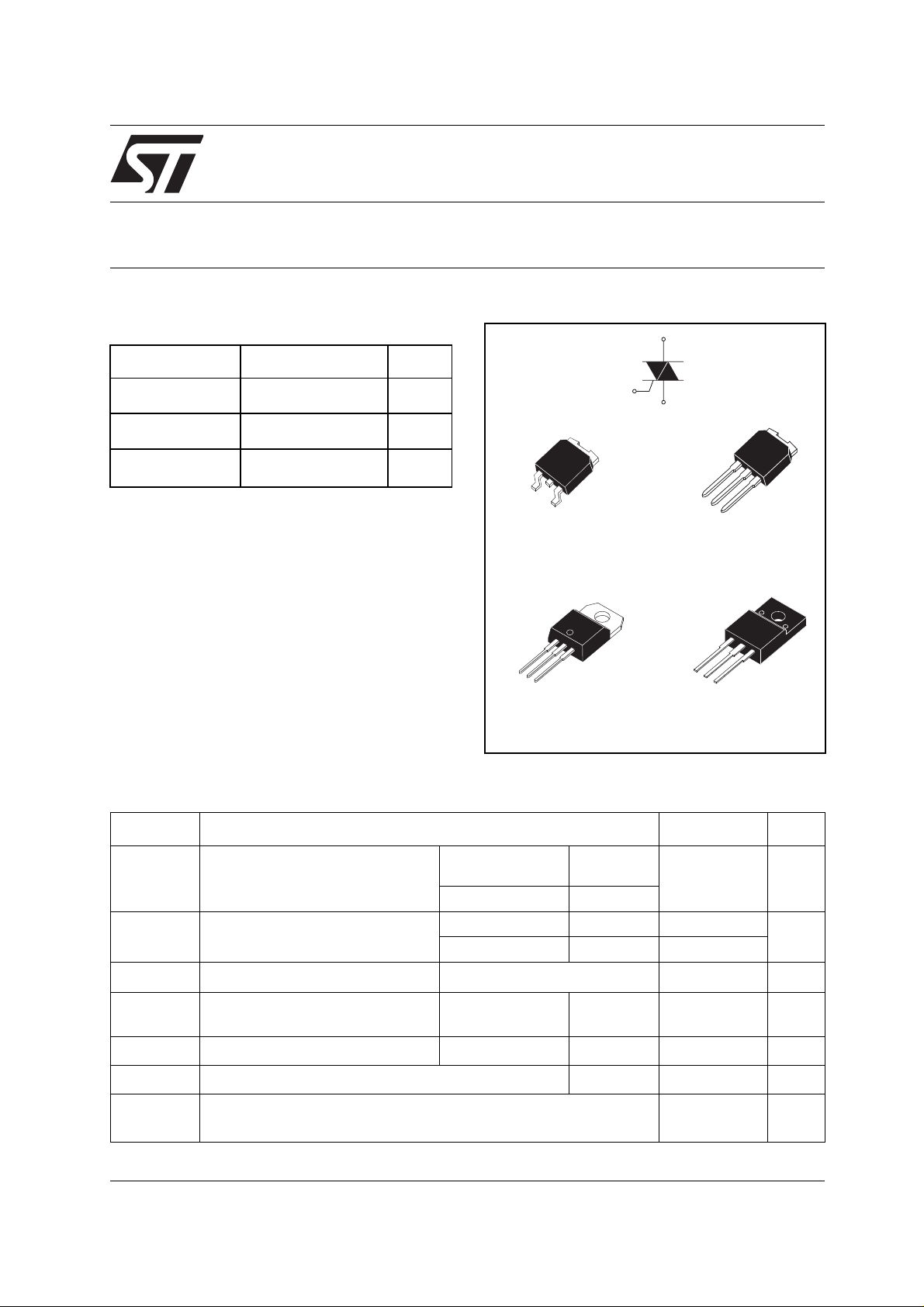
A1
A1
A2
G
A2
A2
G
DPAK
(T4-B)
TO-220AB
(T4-T)
A2
A2
G
A1
A2
A1
A2
G
IPAK
(T4-H)
A1
A2
G
ISOWATT 220AB
(T4-W)
ABSOLUTE MAXIMUM RATINGS
Symbol Parameter Value Unit
I
T(RMS)
I
TSM
²
I
dI/dt
I
GM
P
G(AV)
T
stg
T
June 2003 - Ed: 5
RMS on-state current (full sine wave) DPAK / IPAK
TO-220AB
Tc = 110°C
ISOWATT 220AB Tc = 105°C
Non repetitive surge peak on-state
current (full cycle, Tj initial = 25°C)
tI
²
t Value for fusing
Critical rate of rise of on-state current
= 2 x IGT , tr ≤ 100 ns
I
G
F = 50 Hz t = 20 ms 30 A
F = 60 Hz t = 16.7 ms 31
tp = 10 ms 5.1
F = 120 Hz Tj = 125°C 50 A/µs
Peak gate current tp = 20 µs Tj = 125°C 4 A
Average gate power dissipation Tj = 125°C 1 W
Storage junction temperature range
Operating junction temp erature range
j
- 40 to + 150
- 40 to + 125
4
A
A
°C
²
s
1/8
T4 Series
ELECTRICAL CHARACTERISTICS (Tj = 25°C, unless otherwise specified)
Symbol Test Conditions Quadrant T4
T405 T410 T435
I
GT
V
V
(1)
GT
GD
= 12 V RL = 30 Ω
V
D
VD = V
RL = 33 kΩ
DRM
I - II - III MAX. 5 10 35
I - II - III MAX. 1.3 V
I - II - III MIN. 0.2
Tj = 125°C
(2)
I
H
I
L
= 100 mA
I
T
IG = 1.2 I
GT
MAX. 10 15 35 mA
I - III MAX. 10 25 50 mA
II 15 30 60
dV/dt (2) V
= 67 %V
D
gate open Tj = 125°C
DRM
MIN. 20 40 400 V/µs
(dI/dt)c (2) (dV/dt)c = 0.1 V/µs Tj = 125°C MIN. 1.8 2.7 - A/ms
(dV/dt)c = 10 V/µs Tj = 125°C 0.9 2.0 Without snubber
Tj = 125°C - - 2.5
STATIC CHARACTERISTICS
Symbol Test Conditions Value Unit
I
(2)
V
TM
(2)
V
to
(2)
R
d
I
DRM
I
RRM
Note 1: mi nimum IGT is guaranted at 5% of IGT max.
Note 2: for both polarities of A2 referenced to A1
= 5.5 A tp = 380 µs
TM
Threshold voltage Tj = 125°C MAX. 0.9 V
Dynamic resistance Tj = 125°C MAX. 120 mΩ
V
= V
DRM
RRM
Tj = 25°C MAX. 1.6 V
Tj = 25°C
Tj = 125°C 1 mA
MAX.
5µA
Unit
mA
V
THERMAL RESISTANCES
Symbol Parameter Value Unit
R
th(j-c)
R
th(j-a)
S = Copper surface under tab
T
2/8
Junction to case (AC) DPAK
IPAK
TO-220AB
ISOWATT220AB 4.0
Junction to ambient
S = 0.5 cm
²
DPAK 70
TO-220AB
ISOWATT220AB
IPAK 100
2.6
60
°C/W
°C/W
PRODUCT SELECTOR
T4 Serie s
Part Number
Voltage (xxx)
Sensitivity Type
Package
600 V 700 V 800 V
T405-xxxB X X X 5 mA Logic level DPAK
T405-xxxH X X X 5 mA Logic level IPAK
T405-xxxT X X X 5 mA Logic level TO-220AB
T405-xxxW X X X 5 mA Logic level ISOWATT220AB
T410-xxxB X X X 10 mA Logic level DPAK
T410-xxxH X X X 10 mA Logic level IPAK
T410-xxxT X X X 10 mA Logic level TO-220AB
T410-xxxW X X X 10 mA Logic level ISOWATT220AB
T435-xxxB X X X 35 mA Snubberless DPAK
T435-xxxH X X X 35 mA Snubberle ss IPAK
T435-xxxT X X X 35 mA Snubbe rle ss TO-220AB
T435-xxxW X X X 35 mA Snubberless ISOWATT220AB
ORDERING INFORMA T IO N
T 4 05 - 600 B (-TR)
TRIAC
SERIES
CURRENT:4A
SENSITIVITY:
05: 05mA
10: 10mA
35: 35mA
VOLTAGE:
600: 600V
700: 700V
800: 800V
PACKING MODE:
Blank:Tube
PACKAGE:
B: DPAK
H: IPAK
T:TO-220AB
W: ISOWATT220AB
-TR: DPAK Tape & Reel
OTHER INFORMATION
Part Number Marking Weight
Base
quantity
T4xx-yyyB T4xxyyyB 0.3 g 75 Tube
T4xx-yyyB-TR T4xxyyyB 0.3 g 2500 Tape & reel
T4xx-yyyH T4xxyyy 0.4 g 75 Tube
T4xx-yyyT T4xxyyyT 2.3 g 50 Tube
T4xx-yyyW T4xxyyyW 2.1 g 50 Tube
Note: xx = sensitivity , yyy = voltage
Packing
mode
3/8

T4 Series
Fig. 1: Maximum power dissipation versus RMS
on-state current (full cycle).
P(W)
6
5
4
3
2
1
0
0.0 0.5 1.0 1.5 2.0 2.5 3.0 3.5 4.0
IT(RMS)(A)
Fig. 2-2: RMS on-state current versus ambient
temperature (printed circuit FR4, copper thick-
ness: 35µm),full cycle.
IT(RMS)(A)
2.0
1.8
1.6
1.4
1.2
1.0
0.8
0.6
0.4
0.2
0.0
0 25 50 75 100 125
Tamb(°C)
DPAK
(S=0.5cm²)
Fig. 2-1: RMS on-state current case versus temperature (full cycle).
IT(RMS)(A)
4.5
4.0
3.5
3.0
TO-220AB/DPAK/IPAK
ISOWATT220AB
2.5
2.0
1.5
1.0
0.5
0.0
0 25 50 75 100 125
Tc(°C)
Fig. 3: Relative variation of thermal impedance
versus pulse duration.
K=[Zth/Rth]
1E+0
1E-1
1E-2
1E-2 1E-1 1E+0 1E+1 1E+2 5E+2
Rth(j-c)
TO-220AB/DPAK/IPAK
ISOWATT220AB
Rth(j-a)
TO-220AB/ISOWATT220AB
DPAK/IPAK
tp(s)
Fig. 4: Relative variation of gate trigger current,
holding current and latching current versus
junction temperature (typical values).
IGT,IH,IL [Tj] / IGT,IH,IL [Tj=25°C]
2.5
2.0
1.5
1.0
0.5
0.0
4/8
IGT
IH & IL
Tj(°C)
-40 -20 0 20 40 60 80 100 120 140
Fig. 5: Surge peak on-state current versus
number of cycles.
ITSM(A)
35
30
25
Non repetitive
Tj initial=25°C
20
15
10
5
0
1 10 100 1000
Repetitive
Tc=110°C
Number of cycles
t=20ms
One cycle

T4 Serie s
Fig. 6: Non-repetitive surge peak on-state
current for a sinusoidal pulse with width
tp < 10ms, and corresponding value of I²t.
ITSM (A), I²t (A²s)
500
100
10
dI/dt limitation:
50A/µs
Tj initial=25°C
ITSM
I²t
tp (ms)
1
0.01 0.10 1.00 10.00
Fig. 8: Relative variation of critical rate of
decrease of main current versus (dV/dt)c (typical
values).
(dI/dt)c [(dV/dt)c] / Specified (dI/dt)c
2.4
2.2
2.0
1.8
1.6
1.4
1.2
1.0
0.8
0.6
0.4
0.2
0.0
0.1 1.0 10.0 100.0
(dV/dt)c (V/µs)
T405
T435
T410
Fig. 7: On-state characteristics (maximum
values).
ITM(A)
30.0
10.0
Tj=Tj max.
1.0
Tj max.:
Vto= 0.90 V
Ω
VTM(V)
0.1
0.0 0.5 1.0 1.5 2.0 2.5 3.0 3.5 4.0 4.5 5.0
Rd= 120 m
Fig. 9: Relative variation of critical rate of
decrease of main current versus junction
temperature.
(dI/dt)c [Tj] / (dI/dt)c [Tj specified]
6
5
4
3
2
1
0
0 25 50 75 100 125
Tj(°C)
Fig. 10: DPAK thermal resistance junction to
ambient versus copper surface under tab (printed
circuit board FR4, copper thickness: 35µm).
Rth(j-a) (°C/W)
100
90
80
70
60
50
40
30
20
10
0
0 4 8 1216202428323640
S(cm²)
DPAK
5/8

T4 Series
PACKAGE MECHANICAL DATA
DPAK (Plastic)
DIMENSIONS
R
FOOTPRINT DIMENSIO NS (in millimeters)
DPAK (Plastic)
REF.
A 2.20 2.40 0.086 0.094
A1 0.90 1.10 0.035 0.043
A2 0.03 0.23 0.001 0.009
B 0.64 0.90 0.025 0.035
B2 5.20 5.40 0.204 0.212
C 0.45 0.60 0.017 0.023
C2 0.48 0.60 0.018 0.023
R
D 6.00 6.20 0.236 0.244
E 6.40 6.60 0.251 0.259
G 4.40 4.60 0.173 0.181
H 9.35 10.10 0.368 0.397
L2 0.80 typ. 0.031 typ.
L4 0.60 1.00 0.023 0.039
R 0.2 typ. 0.007 typ.
V2 0° 8° 0° 8°
Millimeters Inches
Min. Max Min. Max.
6.7
6.7
3
3
1.61.6
2.32.3
6/8

PACKAGE MECHANICAL DATA
ISOWATT220AB (Plastic)
T4 Serie s
DIMENSIONS
PACKAGE MECHANICAL DATA
TO-220AB (Plastic)
REF .
Millimeters Inches
Min. Max. Min. Max.
A 4.40 4.60 0.173 0.181
B 2.50 2.70 0.098 0.106
D 2.50 2.75 0.098 0.108
E 0.40 0.70 0.016 0.028
F 0.75 1.00 0.030 0.039
F1 1.15 1.70 0.045 0.067
F2 1.15 1.70 0.045 0.067
G 4.95 5.20 0.195 0.205
G1 2.40 2.70 0.094 0.106
H 10.00 10.40 0.394 0.409
L2 16.00 typ. 0.630 typ.
L3 28.60 30.60 1.125 1.205
L4 9.80 10.60 0.386 0.417
L6 15.90 16.40 0.626 0.646
L7 9.00 9.30 0.354 0.366
Diam 3.00 3.20 0.118 0.126
DIMENSIONS
B
L
I
A
l4
C
b2
F
REF.
A 15.20 15.90 0.598 0.625
a1 3.75 0.147
a2 13.00 14.00 0.511 0.551
B 10.00 10.40 0.393 0.409
b1 0.61 0.88 0.024 0.034
b2 1.23 1.32 0.048 0.051
Millimeters Inches
Min. T yp. Max. Min. Typ. Max.
C 4.40 4.60 0.173 0.181
a1
l3
l2
a2
c2
c1 0.49 0.70 0.019 0.027
c2 2.40 2.72 0.094 0.107
e 2.40 2.70 0.094 0.106
F 6.20 6.60 0.244 0.259
I 3.75 3.85 0.147 0.151
b1
e
M
c1
I4 15.80 16.40 16.80 0.622 0.646 0.661
L 2.65 2.95 0.104 0.116
l2 1.14 1.70 0.044 0.066
l3 1.14 1.70 0.044 0.066
M 2.60 0.102
7/8

T4 Series
PACKAGE MECHANICAL DATA
IPAK (Plastic)
DIMENSIONS
REF.
Millimeters Inches
Min. Typ. Max. Min. Typ. Max.
A
E
B2
L2
C2
A 2.2 2.4 0.086 0.094
A1 0.9 1.1 0.035 0.043
A3 0.7 1.3 0.027 0.051
B 0.64 0.9 0.025 0.035
B2 5.2 5.4 0.204 0.212
B3 0.85 0.033
D
B5 0.3 0.035
B6 0.95 0.037
C 0.45 0.6 0.017 0.023
H
L1
L
B6
B3
B
V1
A1
C2 0.48 0.6 0.019 0.023
D 6 6.2 0.236 0.244
E 6.4 6.6 0.252 0.260
G 4.4 4.6 0.173 0.181
B5
G
C
A3
H 15.9 16.3 0.626 0.641
L 9 9.4 0.354 0.370
L1 0.8 1.2 0.031 0.047
L2 0.8 1 0.031 0.039
V1 10° 10°
Information furnished is believed to be accurate and reliable. However, STMicroelectronics assumes no responsibility for the consequences
of use of su ch in for mat i on n or f or a ny in fr ing em ent of pa te nts or o ther r igh ts of th ir d pa r tie s w hic h may res ul t f rom i ts us e. No license is granted
by impl i cation or ot herwise under any patent or patent ri ghts of STM i croelectro ni cs. Specif i cations mentioned i n this publi cation are subject
to change wi t hout notice. T hi s publicati on supersede s and replaces all in formation previously supplied. STM i croelectro ni cs products are not
authori zed for use as cr i tical compo nents in life support devices or systems without express written approval of STMicroelectronics.
© The ST logo is a registered trademark of STMicroelectronics
© 2003 STMicroelectronics - Printed in It aly - All Rights Reserved
Australi a - Brazil - Chi na - Finland - F rance - Germ any - Hong Kon g - India - Italy - Japan - Mala ysia
Malta - Mor occo - Singapore - Spain - S weden - Switzerland - United Kingdom - U.S. A
STMicroele ct ronics GROUP OF COM PANIES
http://www.st.com
8/8
 Loading...