

STY34NB50F
N - CHANNEL 500V - 0.11Ω - 34 A - Max247
PowerMESH MOSFET
TYPE V
DSS
R
DS(on)
I
D
STY34NB50F 500 V < 0.14 Ω 34 A
■ TYPICALR
■ EXTREMELYHIGH dv/dtCAPABILITY
■ ± 30VGATETO SOURCEVOLTAGERATING
■ 100%AVALANCHETESTED
■ LOW INTRINSICCAPACITANCE
■ GATECHARGE MINIMIZED
■ REDUCEDVOLTAGESPREAD
DS(on)
= 0.11 Ω
DESCRIPTION
Using the latesthigh voltage MESH OVERLAY
process, STMicroelectronics has designed an advanced family of power MOSFETs with outstanding performances. The new patent pending strip
layout coupled with the Company’s proprietary
edge termination structure, gives the lowest
RDS(on) per area, exceptional avalanche and
dv/dt capabilities and unrivalled gate charge and
switchingcharacteristics.
APPLICATIONS
■ HIGHCURRENT, HIGH SPEED SWITCHING
■ SWITCHMODE POWER SUPPLY (SMPS)
■ DC-AC CONVERTERFOR WELDING
EQUIPMENTAND UNINTERRUPTABLE
POWERSUPPLY AND MOTOR DRIVE
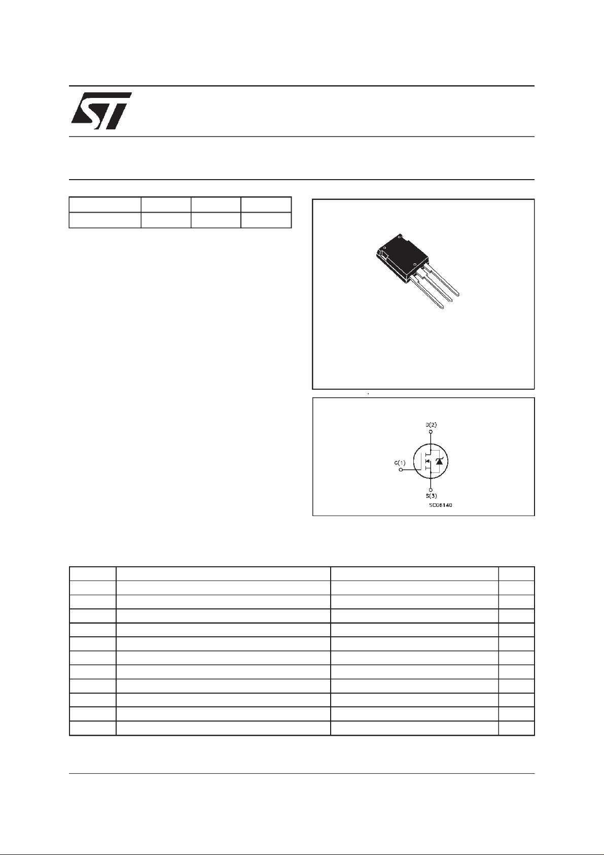
3
2
1
Max247
INTERNAL SCHEMATIC DIAGRAM
ABSOLUTE MAXIMUM RATINGS
Symbol Parameter Value Unit
V
V
V
I
DM
P
dv/dt
T
(•) Pulsewidth limited by safe operating area (1)ISD≤34 A, di/dt ≤ 200 A/µs, VDD≤ V
December 1999
Drain-source Voltage (VGS=0) 500 V
DS
Drain- gate Vo ltage (RGS=20kΩ)
DGR
Gat e-sour ce Voltag e ± 30 V
GS
Drain Curre nt (contin uo us ) at Tc=25oC34A
I
D
Drain Curre nt (contin uo us ) at Tc= 100oC 21.4 A
I
D
500 V
(•) Drain Cu rrent (pulsed) 136 A
Tot al Diss ipation a t Tc=25oC450W
tot
Dera ti ng Factor 3.61 W/
(1) Peak Diode Reco v ery vo lt a ge sl ope 4.5 V/ns
Sto rage T emperat u r e -65 t o 150
stg
Max. Oper at i ng J unction T emper at u r e 150
T
j
(BR)DSS,Tj≤TJMAX
o
C
o
C
o
C
1/8
STY34NB50F
THERMAL DATA
R
thj-case
R
thj-amb
R
thc-sink
T
AVALANCHE CHARACTERISTICS
Symbol Para meter Max V al ue Uni t
I
AR
E
Ther mal Res is t an c e Juncti on-cas e Max
Ther mal Res is t an c e Juncti on-ambient Max
Thermal Resistance Case-sink Typ
Maximum Lead Temperat u re For S old er in g Purpos e
l
Avalanche Cur rent, Repet itiv e or No t -Re petitiv e
(pulse width limited by T
Single Pulse Avalanche Energy
AS
(starting T
=25oC, ID=IAR,VDD=50V)
j
max)
j
0.277
30
0.1
300
34 A
1000 mJ
o
C/W
o
C/W
o
C/W
o
C
ELECTRICAL CHARACTERISTICS (T
=25oC unless otherwisespecified)
case
OFF
Symbol Parameter Test Condit ions Min. Typ. Max. Unit
V
(BR)DSS
Drain-sourc e
=250µAVGS=0
I
D
500 V
Break d own V o lt age
I
DSS
I
GSS
Zero Gate Voltage
Drain Cu rr ent (V
GS
Gat e- b ody Le akage
Current (V
DS
=0)
=0)
V
=MaxRating
DS
= Max Rating Tc=125
V
DS
o
C
= ± 30 V
V
GS
10
100
± 100 nA
ON(∗)
Symbol Parameter Test Condit ions Min. Typ. Max. Unit
V
GS(th)
Gate Threshold
V
DS=VGSID
= 250 µA
345V
Voltage
R
DS(on)
Static Drain-source On
VGS=10V ID= 17 A 0.11 0. 1 4
Resistanc e
I
D(on)
On S t ate Drain Cu rr ent VDS>I
D(on)xRDS(on)max
34 A
VGS=10V
DYNAMIC
Symbol Parameter Test Condit ions Min. Typ. Max. Unit
g
(∗)Forward
fs
Tr ansconduc tance
C
C
C
Input Cap ac i t an c e
iss
Out put Capacita nce
oss
Reverse Transfer
rss
Capacitance
VDS>I
D(on)xRDS(on)maxID
=17A 27 S
VDS=25V f=1MHz VGS=0 5.9
880
80
µA
µ
Ω
nF
pF
pF
A
2/8
STY34NB50F
ELECTRICAL CHARACTERISTICS
(continued)
SWITCHING ON
Symbol Parameter Test Condit ions Min. Typ. Max. Unit
t
d(on)
t
r
Turn-on Time
Rise Time
VDD= 250 V ID=17 A
R
=4.7
G
Ω
VGS=15 V
45
35
(see test circuit, figure 3)
Q
Q
Q
Total Gate Charge
g
Gat e- Source Cha rge
gs
Gate-Drain Charge
gd
VDD= 400 V ID=34A VGS=10V 140
38
61
196 nC
SWITCHING OFF
Symbol Parameter Test Condit ions Min. Typ. Max. Unit
t
r(Voff)
t
t
Off -voltage Rise Time
Fall Time
f
Cross-ov er Time
c
VDD= 400 V ID=17A
R
=4.7
G
Ω
VGS=15V
(see test circuit, figure 5)
28
30
60
SOURCEDRAINDIODE
Symbol Parameter Test Condit ions Min. Typ. Max. Unit
I
V
I
SDM
SD
Q
I
RRM
SD
t
Source-drain Curr ent
(•)
Source-drain Curr ent
34
136
(pulsed)
(∗) Forwar d On Volt age ISD=34A VGS=0 1.6 V
Reverse Recov er y
rr
Time
Reverse Recov er y
rr
=34A di/dt=100A/µs
I
SD
= 100 V Tj=150oC
V
DD
(see test circuit, figure 5)
715
11.8
Charge
Reverse Recov er y
33
Current
ns
ns
nC
nC
ns
ns
ns
A
A
ns
µ
A
C
(∗) Pulsed: Pulse duration = 300 µs, duty cycle 1.5 %
(•) Pulse width limited by safe operatingarea
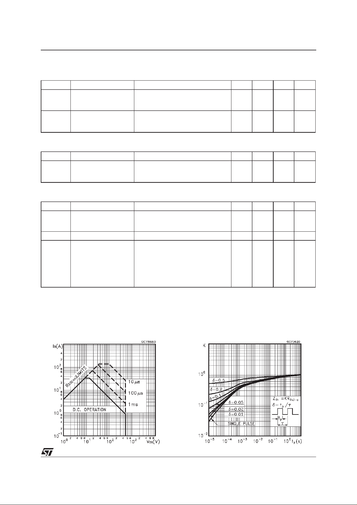
SafeOperating Area ThermalImpedance
3/8

STY34NB50F
OutputCharacteristics
Transconductance
TransferCharacteristics
Static Drain-sourceOn Resistance
Gate Charge vs Gate-sourceVoltage
4/8
CapacitanceVariations

STY34NB50F
Normalized Gate Threshold Voltage vs
Temperature
Source-drainDiode Forward Characteristics
Normalized On Resistancevs Temperature
5/8

STY34NB50F
Fig. 1:
UnclampedInductive Load Test Circuit
Fig. 3: Switching Times Test CircuitsFor
ResistiveLoad
Fig. 2:
UnclampedInductive Waveform
Fig. 4: Gate Charge test Circuit
Fig. 5:
Test CircuitFor InductiveLoad Switching
And Diode Recovery Times
6/8

Max247 MECHANICAL DATA
STY34NB50F
DIM.
MIN. TYP. MAX. MIN. TYP. MAX.
A 4.70 5.30
A1 2.20 2.60
b 1.00 1.40
b1 2.00 2.40
b2 3.00 3.40
c 0.40 0.80
D 19.70 20.30
e 5.35 5.55
E 15.30 15.90
L 14.20 15.20
L1 3.70 4.30
mm inch
P025Q
7/8

STY34NB50F
Information furnished is believed tobeaccurateand reliable.However, STMicroelectronics assumes no responsibility for the consequences
of use of such information nor for any infringement of patents or other rights of third parties which may result from its use. No license is
granted by implication or otherwise under any patent or patent rights ofSTMicroelectronics. Specificationmentioned in this publication are
subjecttochange without notice. This publicationsupersedesandreplaces all information previouslysupplied. STMicroelectronicsproducts
are not authorized for use as critical components in life support devices or systems without express written approval of STMicroelectronics.
The ST logo is a trademark of STMicroelectronics
1999 STMicroelectronics – Printed in Italy – All Rights Reserved
STMicroelectronics GROUP OF COMPANIES
Australia - Brazil - China - Finland - France - Germany - Hong Kong - India - Italy - Japan - Malaysia - Malta - Morocco -
8/8
Singapore - Spain - Sweden - Switzerland - United Kingdom - U.S.A.
http://www.st.com
.
 Loading...