

STY16NA90
N - CHANNEL 900V - 0.5 Ω - 16A - Max247
EXTREMELY LOW GATE CHARGE POWER MOSFET
PRELIMINARY DATA
TYPE V
DSS
ST Y16NA90 900 V < 0. 54 Ω 16 A
R
DS(on)
I
D
■ TYPICALR
■ EFFICIENTANDRELIABLEMOUNTING
DS(on)
=0.5 Ω
THROUGH CLIP
■ ± 30V GATE TO SOURCE VOLTAGERATING
■ REPETITIVEAVALANCHE TESTED
■ LOW INTRINSIC CAPACITANCE
■ 100% AVALANCHETESTED
■ GATECHARGEMINIMIZED
■ REDUCEDTHRESHOLD VOLTAGESPREAD
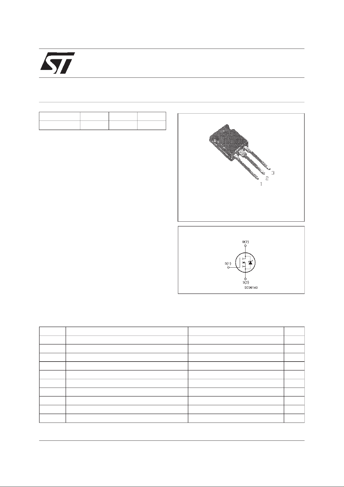
DESCRIPTION
The Max247TMpackage is a new high v olu m e
powe r pac k age ex ibi t ing t he sam e fo ot p rint a s the
indus t r y st andard T O-247, but desi gned to
accomodat e m uch larger s ilicon c hips, normally
suppl ied in bigger packages such as TO-26 4. The
increased die capacity makes the device ideal to
reduce component c ou nt in multiple par a llele d
designs and save board sp ace with respect t o
larger packages .
APPLICATIONS
■ HIGH CURRENT, HIGHSPEEDSWITCHING
■ SWITCHMODEPOWER SUPPLIES(SMPS)
■ DC-ACCONVERTERS FOR WELDING
EQUIPMENTAND UNINTERRUPTIBLE
POWERSUPPLIES (UPS)
Max247
TM
INTERNAL SCHEMATIC DIAGRAM
ABSOLUTE MAXIMUM RATINGS
Symbol Parameter Value Unit
V
V
DGR
V
I
DM
P
T
(•) Pulse width limitedby safe operating area
June 1998
Drain-s ou r ce V oltage (VGS= 0) 900 V
DS
Drain- gat e V oltage (RGS=20kΩ)
Gate-source Voltage ± 30 V
GS
I
Drain Current (continuous) at Tc=25oC16A
D
I
Drain Current (continuous) at Tc=100oC10A
D
900 V
(•) Drain Current (pulsed) 64 A
Tot al Dissipa t io n at Tc=25oC 300 W
tot
Derating Fact or 2.4 W/
Storage Temperature -55 to 150
stg
T
Max. Ope rating Jun ct io n T emperature 150
j
o
C
o
C
o
C
1/5
STY16NA90
THERMAL DATA
R
thj-case
R
thj-amb
R
thc-sin k
AVALANCHE CHARACTERISTICS
Symbol Para met e r Max Value Uni t
I
AR
E
Ther mal Resist ance Junctio n-case Max
Ther mal Resist ance Junctio n-ambient Max
Ther mal Resist ance Case-Heat s ink Typ
with Conduct iv e Grease
Avalanche C ur rent, Rep et it i v e o r Not- Re petitive
(pulse width limited by T
Single Pulse Avalanche Energy
AS
(starting T
=25oC, ID=IAR,VDD=50V)
j
max)
j
0.42
40
0.05
16 A
3000 mJ
o
C/W
o
C/W
ELECTRICAL CHARACTERISTICS (T
=25oC unlessotherwise specified)
case
OFF
Symbol Parameter Test Cond itions Min. Typ. Max. Unit
V
(BR)DSS
Drain-sourc e
=250µAV
I
D
GS
=0
900 V
Breakdown Voltage
I
I
DSS
GSS
Zer o G at e V o lt age
Drain Curre nt ( V
GS
Gat e-body Leak a ge
Current (V
DS
=0)
=0)
V
=MaxRating
DS
=MaxRating Tc=125oC
V
DS
= ± 30 V
V
GS
50
500
± 100 nA
ON (∗)
Symbol Parameter Test Cond itions Min. Typ. Max. Unit
V
GS(th )
Gate Threshold
V
DS=VGSID
=250µA
2.25 3 3.75 V
Voltage
R
DS(on)
Stati c D rain-source On
VGS=10V ID=8A 0.5 0.54 Ω
Resistance
I
D(on)
On Stat e Dra in Curr e nt VDS>I
D(on)xRDS(on)max
16 A
VGS=10V
DYNAMIC
Symbol Parameter Test Cond itions Min. Typ. Max. Unit
g
(∗)Forward
fs
Tr ansconductanc e
C
C
C
Input Ca pac i t an c e
iss
Out put C apa c itance
oss
Reverse T ransfer
rss
Capa cit an c e
VDS>I
D(on)xRDS(on)maxID
=8A 15 S
VDS=25V f=1MHz VGS= 0 6400
600
150
8300
750
200
µA
µA
Ω
pF
pF
pF
2/5
 Loading...