

SGS Thomson Microelectronics STX13005 Datasheet
HIGH VOLTAGE FAST-SWITCHING
Ordering Code Marking Shipment
STX13005
STX13005-AP
■ HIGH VOLTAGE CAPABILITY
■ LOW SPREAD OF DYNAMIC PARAMETERS
■ MINIMUM LOT-TO-LOT SPREAD FOR
RELIABLE OPERATION
■ VERY HIGH SWITCHING SPEED
X13005
X13005
Bulk
Ammopack
STX13005
STX13005-AP
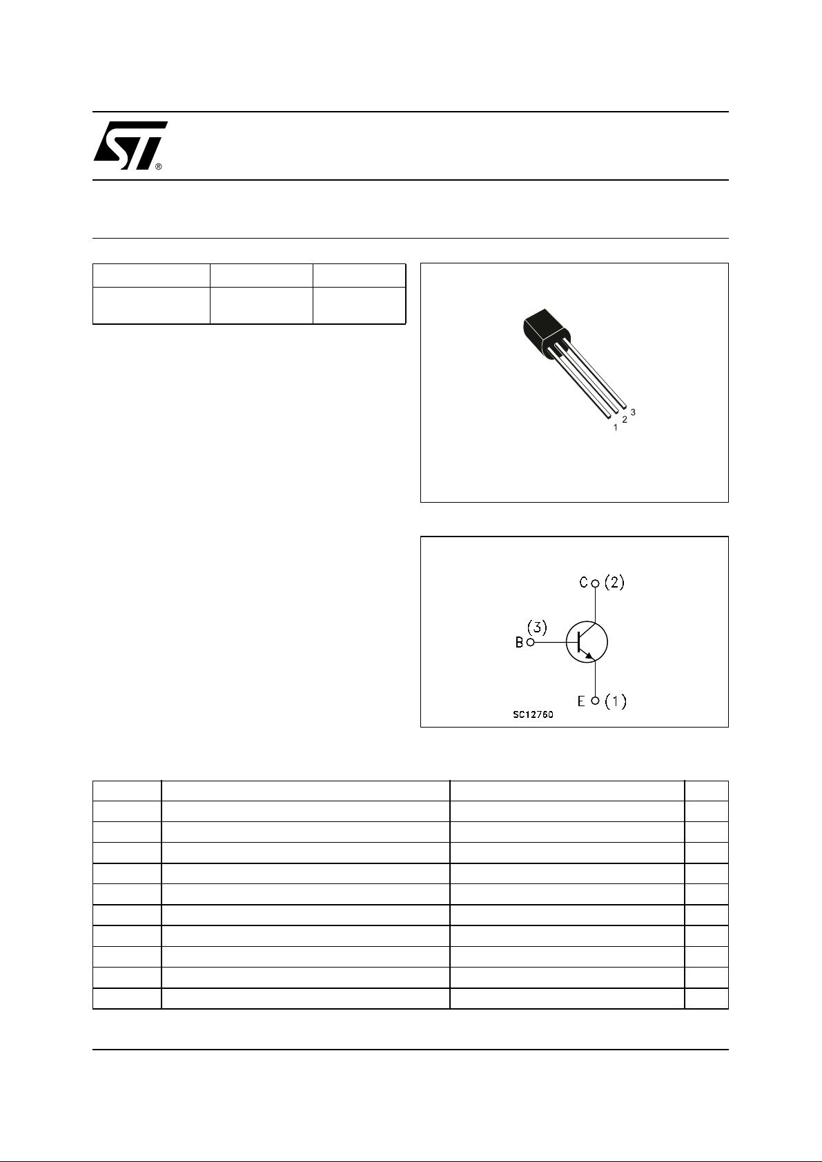
NPN POWER TRANSISTOR
APPLICATIONS:
■ COMPACT FLUORESCENT LAMPS (CFLS)
■ SWITCH MODE POW ER SUPPLIES (AC / DC
TO-92
CONVERTERS)
DESCRIPTION
The device is manu fac tur ed using Hig h V olt age
Multi Epitaxial Planar technology for h igh switching
INTERNAL SCHE MATIC DIAGRAM
speeds and high voltage capability.
It uses a Cellular Emitter structure with planar edge
termination to enhance switching speeds while
maintaining a wide RBSOA.
ABSOLUTE MAXIMUM RATINGS
Symbol Parameter Value Unit
V
CES
V
CEO
V
EBO
I
I
CM
I
I
BM
P
T
stg
T
Collector-Emitter Voltage (VBE=0)
Collector-Emitter Voltage (IB=0)
Emitter-Base Voltage (IC=0,IB< 1.5 A, tp< 10 ms) V
Collector Current 3 A
C
Collector Peak Current (tp< 5 ms)
Base Current 1.5 A
B
Base Peak Current (tp< 5 ms)
Total Dissipation at Tc=25°C
tot
Storage Temperature –65 to 150 °C
Max. Operating Junction Temperature 150 °C
j
700 V
400 V
(BR)EBO
6A
3A
2.8 W
V
1/8November 2002
STX13005 / STX13005- AP
THERMAL DATA
R
thj-case
R
thj-amb
Thermal Resistance Junction-case
Thermal Resistance Junction-ambient
Max
Max
44.6
150
°C/W
°C/W
ELECTRICAL CHARACTE RISTICS (T
= 25 °C unless otherwise spec ified)
j
Symbol Parameter Test Conditions Min. Typ. Max. Unit
I
CES
I
CEO
V
(BR)EBO
Collector Cut-off
Current (V
BE
=0)
Collector Cut-off
Current (I
B
=0)
Emitter-Base
V
= 700 V
CE
VCE= 700 V
V
= 400 V 1 mA
CE
=10mA 9 18 V
I
E
=100°C
T
j
1
5
Breakdown Voltage
=0)
(I
C
V
CEO(sus)
* Collector-Emitter
I
= 10 mA 400 V
C
Sustaining Voltage
=0)
(I
B
* Collector-Emitter
V
CE(sat)
Saturation Voltage
* Base-Emitter
V
BE(sat)
Saturation Voltage
hFE* DC Current Gain IC=1A
RESISTIVE LOAD
s
f
Storage Time
Fall Time
t
t
INDUCTIVE LOAD
s
f
Storage Time
Fall Time
t
t
IC=1A
IC=2A
I
=3A
C
IC=1A
=2A
I
C
=2A
I
C
IC=2A
I
=-IB2= 400 mA
B1
(See Figure 1)
IC=1A
= 200 mA
I
B1
L = 50 mH
=200mA
I
B
IB=500mA
I
=750mA
B
I
=200mA
B
=500mA
I
B
V
=5V
CE
=5V
V
CE
= 125 V
V
CC
t
=30µs
p
V
= 300 V
clamp
=-5V
V
BE(off)
R
=0
BB
10
0.5
0.6
5
1.2
1.6
30
8
24
1.65
260
0.8
150
(See Figure 2)
* Pulsed:Pulse duration= 300 µs,duty cycle=1.5 %.
mA
mA
V
V
V
V
V
µs
ns
µs
ns
2/8
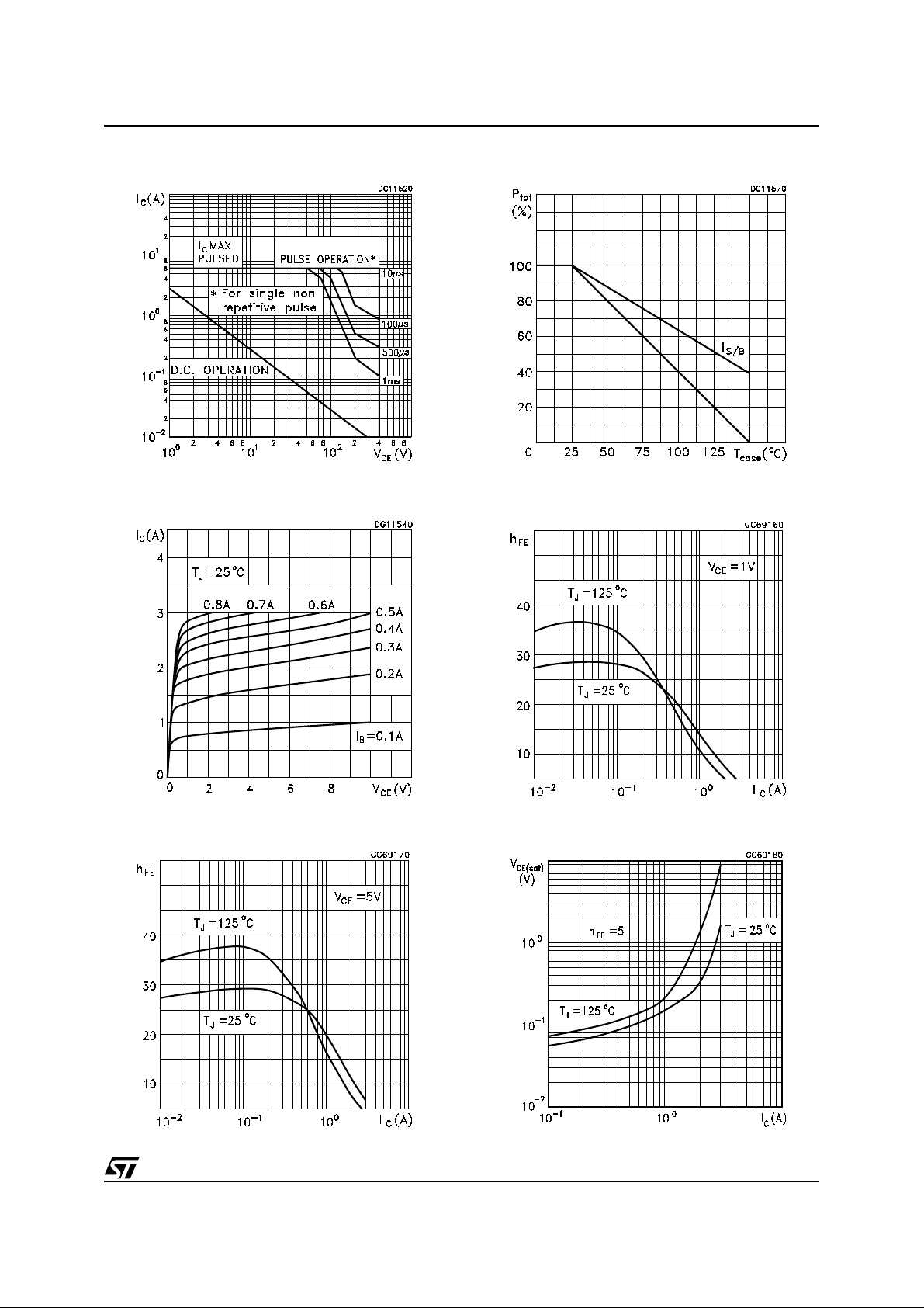
Safe Operating Area Derating Curve
DC Cu rrent GainOutput Characteristics
STX13005 / STX13005- A P
DC Current Gain
Collector-Emitter Saturation Voltage
3/8
 Loading...