

®
■ MONOLI THIC D A RLING TO N
CONFIGU R ATIO N
■ INTEGRATED ANTIPARALLEL
COLLECTOR-EMITTER DIODE
APPLICATIONS
■ LINEAR AND SWITCHING INDUSTRIAL
EQUIPMENT
DESCRIPTION
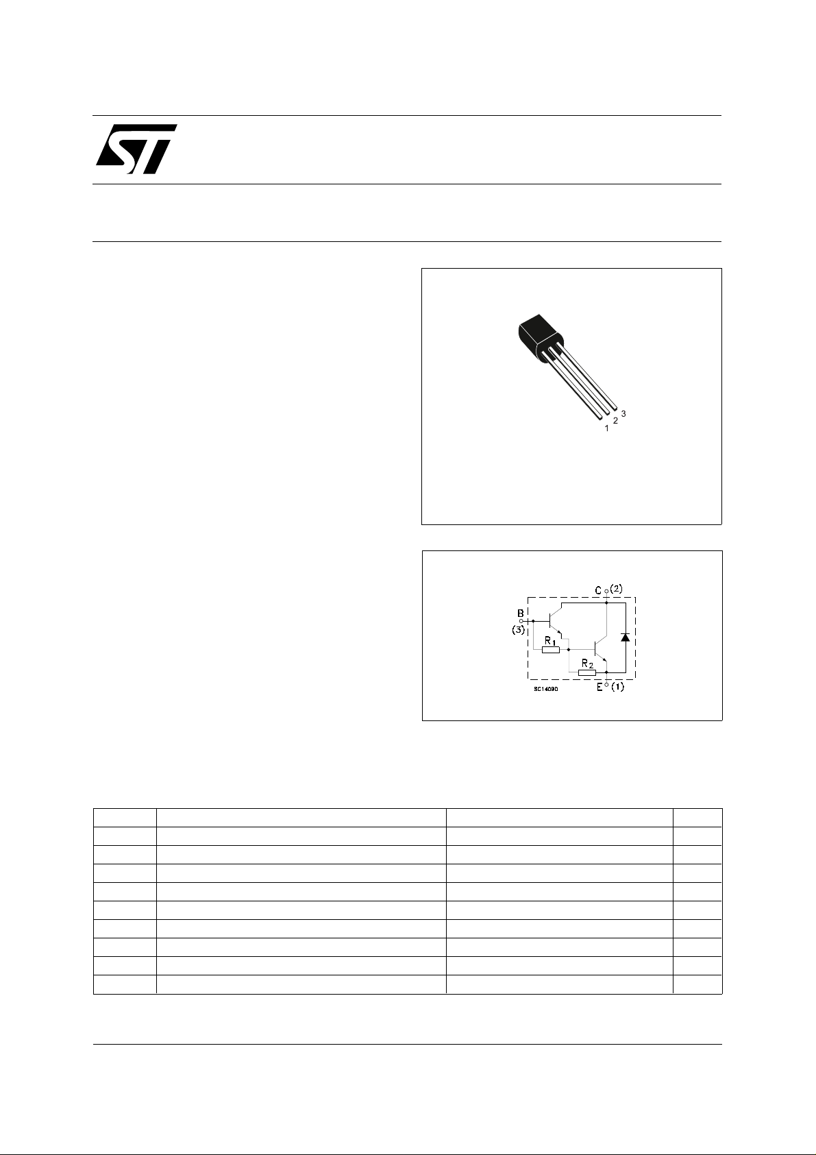
The device is a silicon Epitaxial-Base NPN
transistor in monolithic Darlington configuration
mounted in TO-92 plastic package. It is intented
for use in linear and switching applications.
Ordering codes:
STX112 (shipment in bulk)
STX112-AP (shipment in ammopack)
STX112
SILICON NPN POWER
DARLINGTON TRANSISTOR
TO-92
INTER NAL SCH E M ATI C DIAG RA M
R1 Typ.= 7K Ω R2 Typ.= 230
ABSOLUTE MAXIMUM RATINGS
Symbol Parameter Value Unit
V
V
V
I
P
T
October 2000
Collector-Base Voltage (IE = 0) 100 V
CBO
Collector-Emitter Voltage (IB = 0) 100 V
CEO
Emitter-Base Voltage (IC = 0) 5 V
EBO
Collector Current 2 A
I
C
Collector Peak Current 4 A
CM
Base Current 50 mA
I
B
Total Dissipation at T
tot
Storage Temperature -65 to 150
stg
T
Max. Operating Junction Temperature 150
j
= 25 oC 1.2 W
amb
o
C
o
C
1/5
STX112
THERMAL DATA
R
thj-amb
Thermal Resistance Junction-ambient Max 104
o
C/W
ELECTRICAL CHARACTERISTICS (T
= 25 oC unless otherwise specified)
case
Symbol Parameter Test Conditions Min. Typ. Max. Unit
I
CEO
I
CBO
I
EBO
V
CEO(sus)
Collector Cut-off
Current (I
= 0)
B
Collector Cut-off
Current (I
= 0)
E
Emitter Cut-off Current
(I
= 0)
C
∗ Collector-Emitter
= 50 V 2 mA
V
CE
= 100 V 1 mA
V
CB
= 5 V 2 mA
V
EB
I
= 30 mA 100 V
C
Sustaining Voltage
(I
= 0)
B
∗ Collector-Emitter
V
CE(sat)
IC = 2 A IB = 8 mA 2.5 V
Saturation Voltage
∗ Base-Emitter Voltage IC = 2 A VCE = 4 V 2.8 V
V
BE
hFE∗ DC Current Gain IC = 1 A VCE = 4 V
I
= 2 A VCE = 4 V
C
∗ Pulsed: Pulse duration = 300 µs, duty cycle 1.5 %
1000
500
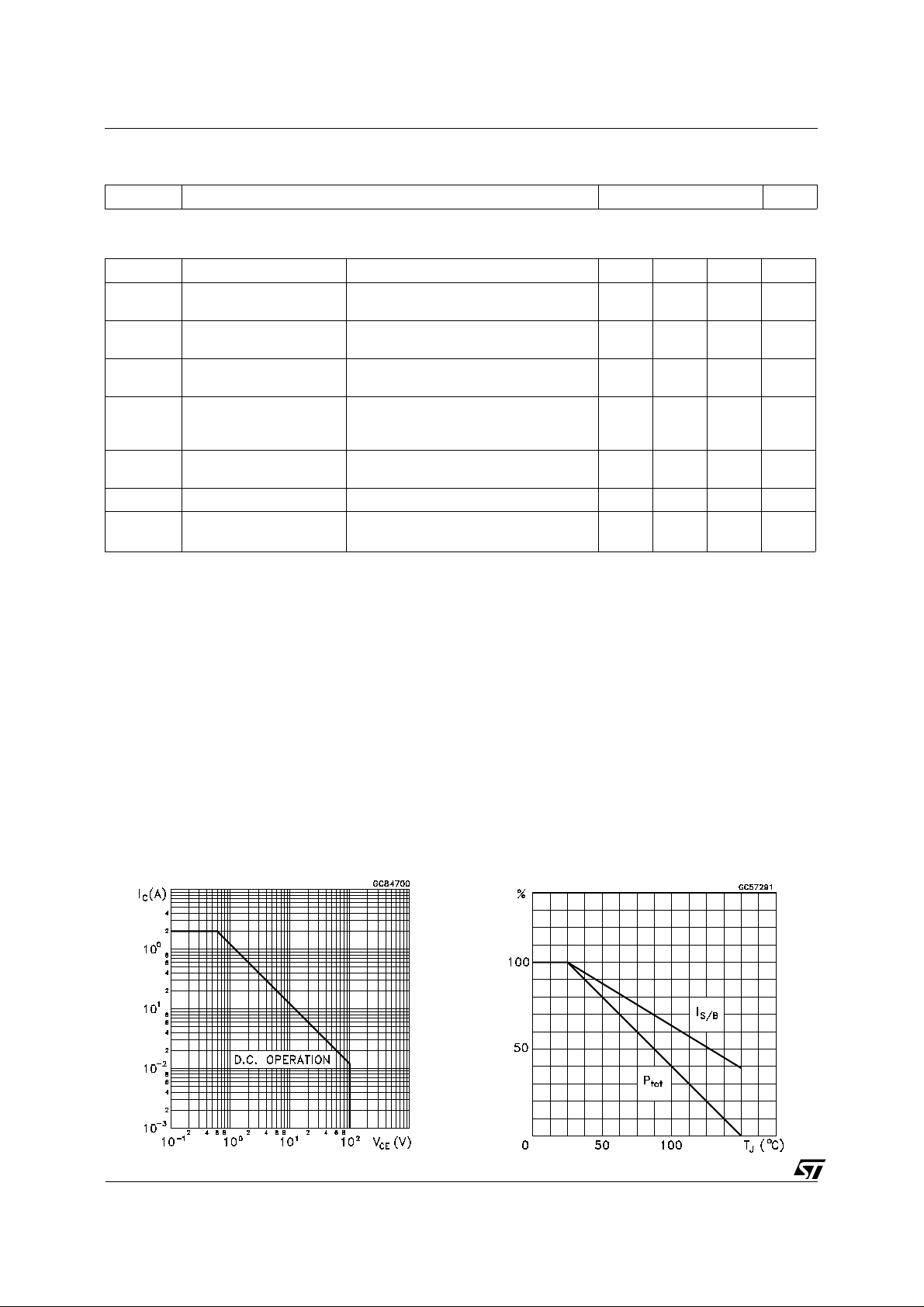
Safe Operating Are a Derating Curve
2/5

STX112
DC Current Gain
Base-Em itter Sat uration Volt a ge
Collector-Emitt er Sat uration Volta ge
Base-Emitt er On Voltag e
Freewheel Diode Forward Voltage
3/5

STX112
TO-92 MECHANICAL DATA
DIM.
MIN. TYP. MAX. MIN. TYP. MAX.
A 4.58 5.33 0.180 0.210
B 4.45 5.2 0.175 0.204
C 3.2 4.2 0.126 0.165
D 12.7 0.500
E1.27 0.050
F 0.4 0.51 0.016 0.020
G0.35 0.14
mm inch
4/5

STX112
Information furnished is believed to be accurate and reliable. However, STMicroelectronics assumes no responsibility for the consequences
of use of such inform ation nor for any infringe ment o f patents or other rig hts o f third par ties which ma y resul t from i ts use. N o li cen se is
granted by implicatio n or otherwise under any patent or patent rights of STMicroelectronics. Specification mentioned in this publication are
subject to change without notice. This publication supersedes and replaces all information previously supplied. STMicroelectronics products
are not authorized for use as critical compo nents in life support devices or systems without express written approval of STMicroelectronics.
The ST logo is a trademark of STMicroelectronics
© 2000 STMicroelectro nics – Printed in Italy – All Rights Reserved
STMicroelectronics GROUP OF COMPANIES
Australia - Brazil - China - Finland - France - Germany - Hong Kong - India - Italy - Japan - Malaysia - Malta - Morocco -
Singapore - Spain - Sweden - Switzerland - United Kingdom - U.S.A.
http://www.st.com
5/5
 Loading...