

STW34NB20
N - CHANNEL ENHANCEMENT MODE
PowerMESH MOSFET
TYPE V
DSS
R
DS(on)
I
D
ST W34NB20 200 V < 0.07 5 Ω 34 A
■ TYPICALR
■ EXTREMELY HIGH dv/dt CAPABILITY
■ 100% AVALANCHETESTED
■ VERYLOW INTRINSICCAPACITANCES
■ GATECHARGEMINIMIZED
DS(on)
=0.062 Ω
DESCRIPTION
Using the latesthigh voltage MESH OVERLAY
process, SGS-Thomson has designed an
advanced family of power MOSFETs with
outstanding performances. The new patent
pending strip layout coupled with the Company’s
proprietary edge termination structure, gives the
lowest R
per area, exceptional avalanche
DS(on)
and dv/dt capabilities and unrivalled gate charge
and switching characteristics.
APPLICATIONS
■ SWITCHMODEPOWER SUPPLIES(SMPS)
■ DC-ACCONVERTERS FORWELDING
EQUIPMENTAND UNINTERRUPTIBLE
POWERSUPPLIES AND MOTORDRIVE
■ HIGH CURRENT, HIGH SPEEDSWITCHING
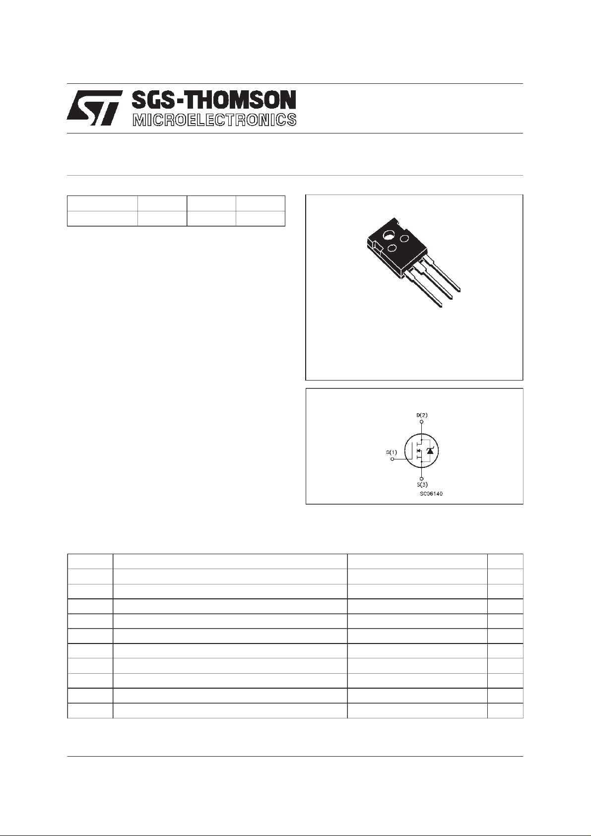
3
2
1
TO-247
INTERNAL SCHEMATIC DIAGRAM
ABSOLUTE MAXIMUM RATINGS
Symb o l Para meter Value Uni t
V
V
V
I
DM
P
T
(•) Pulsewidth limitedby safe operating area (1)ISD≤34A, di/dt ≤ 200 A/µs, VDD≤ V
January 1998
Drain-source Voltage (VGS=0) 200 V
DS
DGR Drain- gate Voltage ( R
Gat e- source Voltage ± 30 V
GS
I
Drain Current (con t in uous) at Tc=25oC34A
D
I
Drain Current (con t in uous) at Tc=100oC21A
D
=20kΩ)
GS
200 V
(•) Dra in Current (pulsed) 136 A
Tot al Dissipat i on at Tc=25oC180W
tot
Derating Factor 1.44 W/
Sto rage Tem pe r ature -65 to 150
stg
T
Max. Operat ing Ju nc t io n Temper at u r e 150
j
,Tj≤T
(BR)DSS
JMAX
o
C
o
C
o
C
1/8

STW34NB20
THERMAL DATA
R
thj-case
Rthj-amb
R
thc-sin k
T
AVALANCHE CHARACTERISTICS
Symbol Para met e r Max Va lue Uni t
I
AR
E
Ther mal Resist ance Junction-c a s e Max
Ther mal Resist ance Junction-ambient Max
Ther mal Resist ance Case-sink Typ
Maximum Lead Te mperatu re Fo r Soldering Purpos e
l
Avalanche Curre nt, Repet it ive o r Not-Repetitive
(pulse w idth limited by T
Single Pulse Avalanche Energy
AS
(starting T
=25oC, ID=IAR,VDD=50V)
j
max, δ <1%)
j
0.69
30
0.1
300
34 A
650 mJ
o
C/W
oC/W
o
C/W
o
C
ELECTRICAL CHARACTERISTICS (T
=25oC unlessotherwise specified)
case
OFF
Symbol Parameter Test Condition s Min. Typ. M ax. Unit
V
(BR)DSS
Drain-source
=250µAVGS=0
I
D
200 V
Breakdown Volt age
I
DSS
I
GSS
Zer o Gate Vo lt age
Drain Cur rent (V
GS
Gat e-body Leakage
Current (V
DS
=0)
=0)
=MaxRating
V
DS
V
=MaxRating Tc=125oC
DS
= ± 30 V
V
GS
1
10
± 100 nA
ON (∗)
Symbol Parameter Test Condition s Min. Typ. M ax. Unit
V
GS(th )
Gate Threshold
V
DS=VGSID
=250µA
345V
Voltage
R
DS(on)
Stati c Drain-so urce On
VGS=10V ID=17 A 0.062 0. 075 Ω
Resistance
I
D(on)
On State D ra in Current VDS>I
D(on)xRDS(on)max
34 A
VGS=10V
DYNAMIC
Symbol Parameter Test Condition s Min. Typ. M ax. Unit
g
(∗)Forward
fs
Tr ansconductance
C
C
C
Input Capaci t an ce
iss
Out put Capac itance
oss
Reverse Transfer
rss
Capa cit an c e
VDS>I
D(on)xRDS(on)maxID
=17A 8 17 S
VDS=25V f=1MHz VGS= 0 2400
650
90
3300
900
130
µA
µA
pF
pF
pF
2/8
STW34NB20
ELECTRICAL CHARACTERISTICS (continued)
SWITCHINGON
Symbol Parameter Test Condition s Min. Typ. M ax. Unit
t
d(on)
Turn-on Time
r
Rise Time
t
VDD=100V ID=17A
=4.7 Ω VGS=10V
R
G
30
40
(see test circuit, figure 3)
Q
Q
Q
Total Gate Charge
g
Gat e-Source Charge
gs
Gate-Drain Charge
gd
VDD=160V ID=34 A VGS=10V 60
19
29
SWITCHINGOFF
Symbol Parameter Test Condition s Min. Typ. M ax. Unit
t
r(Voff)
t
t
Of f - voltage Rise Time
Fall Time
f
Cross-over Tim e
c
VDD=160V ID=34A
=4.7 Ω VGS=10V
R
G
(see test circuit, figure 5)
17
18
35
SOURCE DRAIN DIODE
Symbol Parameter Test Condition s Min. Typ. M ax. Unit
I
SD
I
SDM
V
SD
t
Q
I
RRM
(∗) Pulsed: Pulse duration =300 µs, duty cycle 1.5 %
(•) Pulse widthlimited by safe operating area
Source-drain Current
(•)
Source-drain Current
(pulsed)
(∗) For ward On Voltage ISD=34A VGS=0 1.5 V
Reverse R ec overy
rr
Time
Reverse R ec overy
rr
= 34 A di/dt = 100 A/µs
I
SD
=50V Tj=150oC
V
DD
(see test circuit, figure 5)
Charge
Reverse R ec overy
Current
40
55
80 nC
23
24
47
34
136
290
2.7
18.5
ns
ns
nC
nC
ns
ns
ns
A
A
ns
µC
A
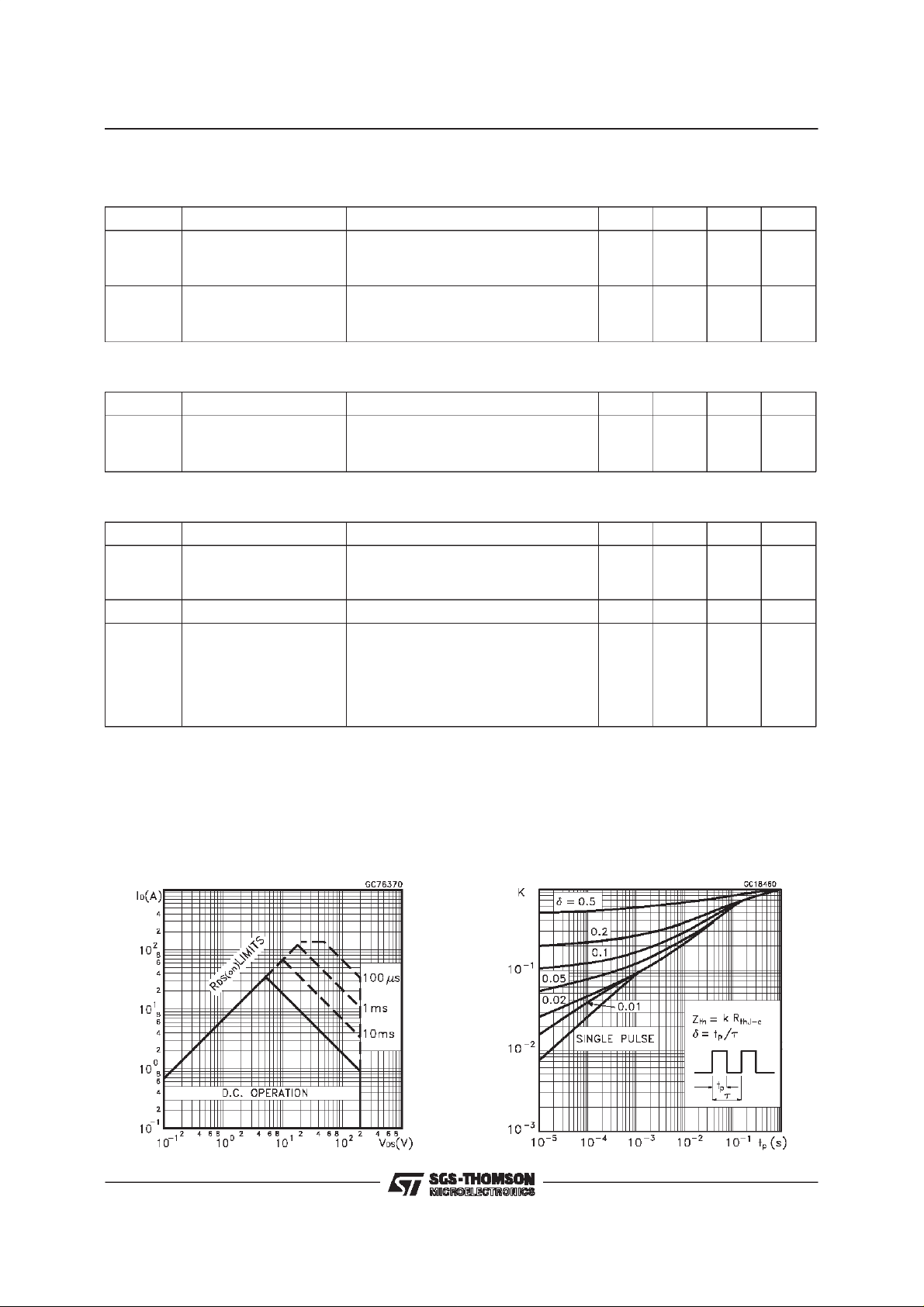
Safe Operating Area ThermalImpedance
3/8

STW34NB20
OutputCharacteristics
Transconductance
TransferCharacteristics
StaticDrain-sourceOn Resistance
GateCharge vs Gate-sourceVoltage
4/8
CapacitanceVariations

STW34NB20
Normalized GateThresholdVoltage vs
Temperature
Source-drainDiode ForwardCharacteristics
Normalized On Resistancevs Temperature
5/8

STW34NB20
Fig. 1: UnclampedInductiveLoad Test Circuit
Fig. 3: Switching Times Test CircuitsFor
ResistiveLoad
Fig. 2: UnclampedInductive Waveform
Fig. 4: Gate Charge test Circuit
Fig. 5: Test Circuit For Inductive Load Switching
And Diode RecoveryTimes
6/8

TO-247 MECHANICAL DATA
STW34NB20
DIM.
MIN. TYP. MAX. MIN. TYP. MAX.
A 4.7 5.3 0.185 0.209
D 2.2 2.6 0.087 0.102
E 0.4 0.8 0.016 0.031
F 1 1.4 0.039 0.055
F3 2 2.4 0.079 0.094
F4 3 3.4 0.118 0.134
G 10.9 0.429
H 15.3 15.9 0.602 0.626
L 19.7 20.3 0.776 0.779
L3 14.2 14.8 0.559 0.413 0.582
L4 34.6 1.362
L5 5.5 0.217
M 2 3 0.079 0.118
Dia 3.55 3.65 0.140 0.144
mm inch
P025P
7/8

STW34NB20
Information furnished is believed tobeaccurate and reliable. However, SGS-THOMSON Microelectronics assumes no responsability for the
consequences of use of such information nor for any infringement of patents or other rightsof third parties which may results from its use. No
license is granted by implication or otherwiseunder any patent or patent rights of SGS-THOMSON Microelectronics. Specifications mentioned
in thispublication are subjectto change without notice. This publication supersedes and replaces all information previously supplied.
SGS-THOMSON Microelectronics products are not authorized for useas criticalcomponentsin life support devices orsystems withoutexpress
written approval ofSGS-THOMSON Microelectonics.
1998 SGS-THOMSON Microelectronics - Printed in Italy -All RightsReserved
Australia - Brazil - Canada - China - France - Germany- Italy - Japan - Korea - Malaysia - Malta - Morocco - The Netherlands -
Singapore - Spain - Sweden - Switzerland - Taiwan - Thailand - United Kingdom -U.S.A
8/8
SGS-THOMSON MicroelectronicsGROUP OF COMPANIES
...
 Loading...