

SGS Thomson Microelectronics STW15NA50, STH15NA50FI Datasheet
STH15NA50/FI
STW15NA50
N - CHANNEL ENHANCEMENT MODE
FAST POWER MOS TRANSISTOR
TYPE V
STH 15NA50
STH 15NA50FI
STW15NA50
■ TYPICAL R
■ ± 30V GATE TO SOURCE VOLTAGE RATING
■ 100% AVALANCHE TESTED
■ REPETITIVE AVALANCHE DATA AT 100
■ LOW INTRINSIC CAPACITANCES
■ GATE GHARGE MINIMIZED
■ REDUCED THRESHOLD VOLTAGE SPREAD
DS(on)
DSS
500 V
500 V
500 V
= 0.33 Ω
R
DS(on)
<0.4Ω
<0.4Ω
<0.4Ω
I
D
14.6 A
9.3 A
14.6 A
o
C
DESCRIPTION
This series of POWER MOSFETS represents the
most advanced high voltage technology. The optimized cell layout coupled with a new proprietary
edge termination concur to give the device low
R
and gate charge, unequalled ruggedness
DS(on)
and superior switching performance.
APPLICATIONS
■ HIGH CURRENT, HIGH SPEED SWITCHING
■ SWITCH MODE POWERSUPPLIES (SMPS)
■ DC-AC CONVERTERS FOR WELDING
EQUIPMENT AND UNINTERRUPTIBLE
POWER SUPPLIES AND MOTOR DRIVE
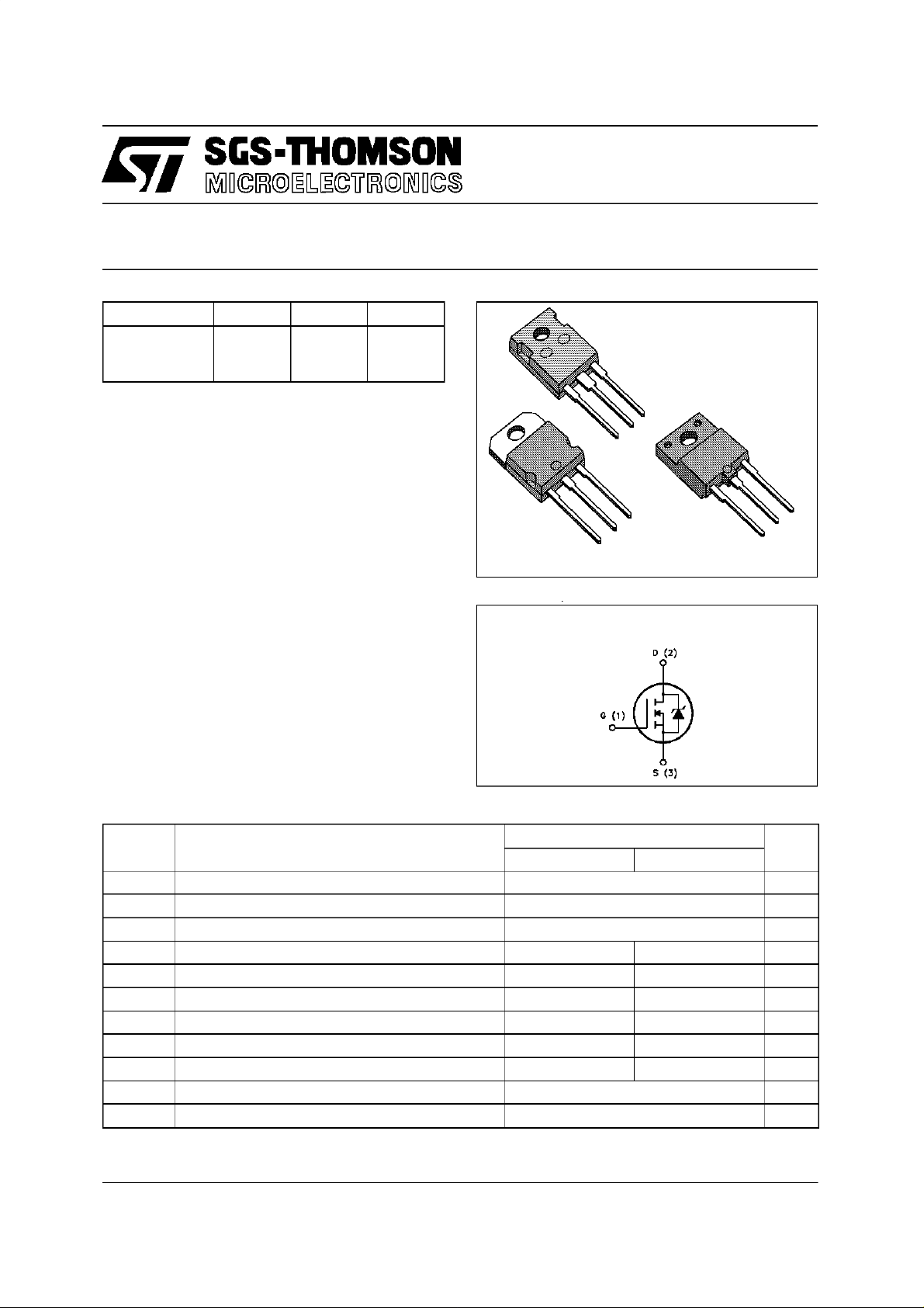
TO-247
3
2
1
3
2
TO-218 ISOWATT218
1
INTERNAL SCHEMATIC DIAGRAM
3
2
1
ABSOLUTE MAXIMUM RATINGS
Symb o l Paramet er Val u e Unit
ST H/STW15NA50 STH 15NA50FI
V
V
V
I
DM
P
V
T
(•) Pulsewidth limited bysafe operating area
November 1996
Drain - s ource Voltage (VGS=0) 500 V
DS
Drain- gate Voltage (RGS=20kΩ)500V
DGR
Gate-source Voltage ± 30 V
GS
Drain Current (continuous) at Tc=25oC14.69.3A
I
D
Drain Current (continuous) at Tc=100oC9.2 5.5A
I
D
(•) Drain Current (pulsed) 58.4 58.4 A
Total Di ssipation at Tc=25oC 190 80 W
tot
Derat ing Factor 1.52 0.64 W/
Ins ulation Withs t and Voltage (DC) 4000 V
ISO
St or a ge Tem perature -65 to 150
stg
Max. Operating Junction Temperature 150
T
j
o
o
o
C
C
C
1/11

STH15NA50/FI - STW15NA50
THERMAL DATA
TO - 218/ TO-247 IS OWATT218
R
thj-case
R
thj-amb
R
thc-sink
T
AVALANCHE CHARACTERISTICS
Symbol Parameter Max Value Uni t
I
AR
E
E
I
AR
Thermal Resistance Junction - cas e Max 0.66 1.56
Thermal Resistance Junction- ambient Max
Thermal Resistance Case-sink Typ
Maximum Lead T emperature For Soldering Purpose
l
Avalanc h e Cu rr ent , Repet itive or Not-R ep et itive
(pulse width limited by Tjmax, δ <1%)
Single Pul se Avalanche Ener gy
AS
(starti ng T
Repetitive Avalanc he Energ y
AR
=25oC, ID=IAR,VDD=50V)
j
(pulse width limited by Tjmax, δ <1%)
Avalanc h e Cu rr ent , Repet itive or Not-R ep et itive
(Tc= 100oC, pulse width limited by Tjmax, δ <1%)
30
0.1
300
14.6 A
850 mJ
30 mJ
9.2 A
o
C/W
o
C/W
o
C/W
o
C
ELECTRICAL CHARACTERISTICS (T
=25oC unless otherwise specified)
case
OFF
Symbol Parameter Test Co ndition s Min. Typ. Max. Unit
V
(BR)DSS
Drain - s ource
ID=250µAVGS= 0 500 V
Break d own Volta ge
I
DSS
I
GSS
Zer o Gate Volt age
Drain Current (VGS=0)
Gat e- body Leak age
Current (V
DS
=0)
VDS=MaxRating
VDS= Max Rating x 0 .8 Tc=125oC
= ± 30 V ± 100 nA
V
GS
25
250
ON (∗)
Symbol Parameter Test Co ndition s Min. Typ. Max. Unit
V
GS(th)
R
DS(on)
Gate Threshold Voltage VDS=VGSID=250µA 2.25 3 3.75 V
St at ic Drain-s our ce O n
VGS=10V ID= 7.5 A 0.33 0.4 Ω
Resistance
I
D(on)
On State Drain Current VDS>I
D(on)xRDS(on)max
14.6 A
VGS=10V
DYNAMIC
Symbol Parameter Test Co ndition s Min. Typ. Max. Unit
(∗)Forward
g
fs
Tr ansconductance
C
C
C
Input Capacitance
iss
Out put Capacitance
oss
Reverse Transfer
rss
Capacitance
VDS>I
D(on)xRDS(on)maxID
=7.5A 9 13 S
VDS=25V f=1MHz VGS= 0 2500
345
105
3250
450
140
µA
µA
pF
pF
pF
2/11
STH15NA50/FI - STW15NA50
ELECTRICAL CHARACTERISTICS (continued)
SWITCHING ON
Symbol Parameter Test Co ndition s Min. Typ. Max. Unit
t
d(on)
(di/dt)
Q
Q
Q
Turn-on T im e
t
Rise Time
r
Turn-on C urrent S lope VDD=400V ID=15A
on
Total Gate Charge
g
Gat e- Source Charge
gs
Gate-Drain Charge
gd
SWITCHING OFF
Symbol Parameter Test Co ndition s Mi n. Typ. Max. Unit
t
r(Voff)
t
Off -voltage R ise Time
t
Fall Time
f
Cross-over Time
c
SOURCE DRAIN DIODE
VDD=225V ID=7.5A
RG=4.7 Ω VGS=10V
24
37
(see test circuit, figure 3)
225 A/µs
RG=47 Ω VGS=10V
(see test circuit, figure 5)
VDD= 400 V ID=15A VGS=10V 110
15
55
VDD=400V ID=15A
RG=4.7 Ω VGS=10V
(see test circuit, figure 5)
25
17
45
34
50
140 nC
35
24
60
ns
ns
nC
nC
ns
ns
ns
Symbol Parameter Test Co ndition s Mi n. Typ. Max. Unit
I
I
SDM
SD
Source-drain Current
(•)
Source-drain Current
14.6
58.4
(pulsed)
V
(∗) Forward On Volt age ISD=15A VGS=0 1.6 V
SD
t
Reverse Recovery
rr
Time
Q
Reverse Recovery
rr
ISD= 15 A di/dt = 100 A/µs
VDD= 100 V Tj=150oC
(see test circuit, figure 5)
640
12.8
Charge
I
RRM
Reverse Recovery
40
Current
(∗) Pulsed:Pulse duration = 300 µs, dutycycle 1.5 %
(•) Pulse widthlimited by safeoperating area
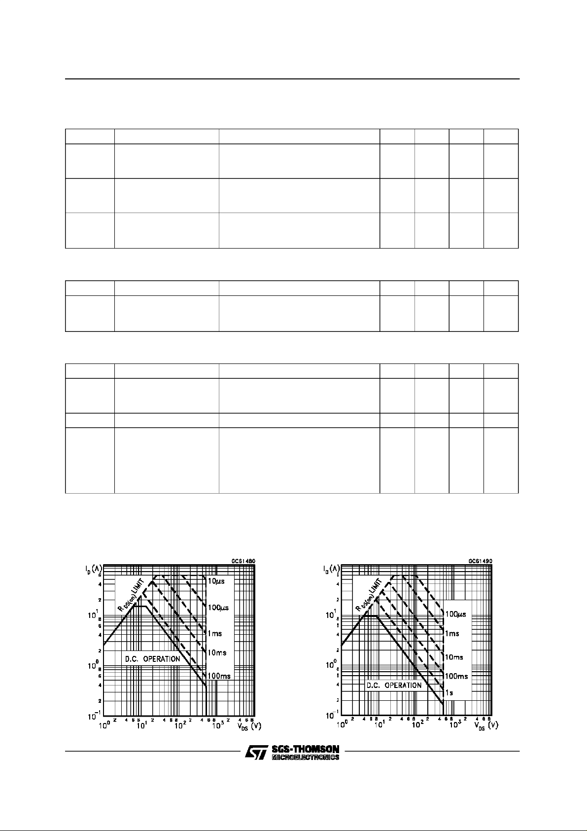
Safe Operating Areas For TO-218 and TO-247 Safe Operating Areas For ISOWATT218
A
A
ns
µC
A
3/11
STH15NA50/FI - STW15NA50
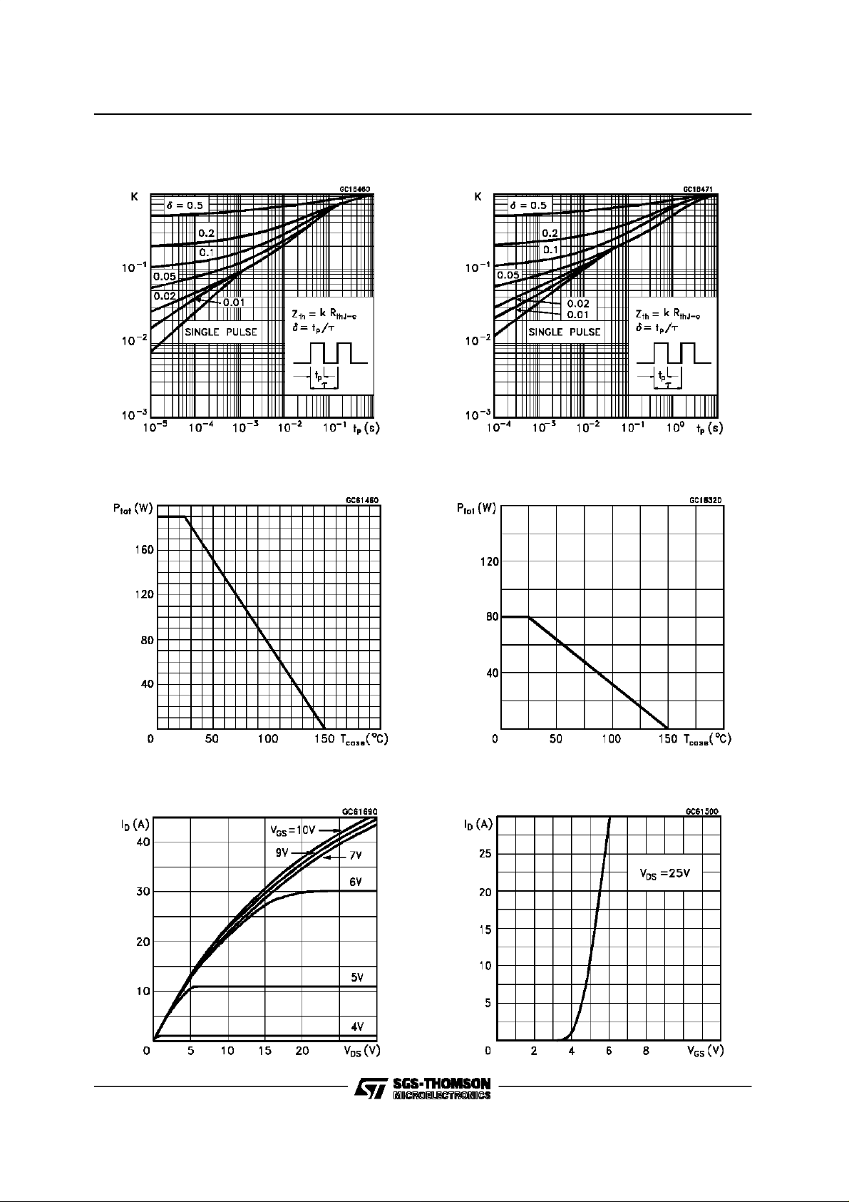
Thermal ImpedeanceFor TO-218 and TO-247
Derating Curve For TO-218 and TO-247
Thermal Impedance For ISOWATT218
Derating Curve For ISOWATT218
Output Characteristics
4/11
Transfer Characteristics
 Loading...