

SGS Thomson Microelectronics STW14NM50 Datasheet
STW14NM50
N-CHANNEL 500V - 0.32Ω - 14A TO-247
MDmesh™Power MOSFET
PRELIMINARY DATA
TYPE V
DSS
R
DS(on)
I
D
STW14NM50 500V < 0.35Ω 14 A
■ TYPICAL R
■ HIGH dv/dt AND AVALANCHE CAPABILITIES
■ 100% AVALANCHE TESTED
■ LOW INPUT CAPACITANCE AND GATE
(on) = 0.32Ω
DS
CHARGE
■ LOW GATE INPUT RESIST ANC E
■ TIGHT PROCESS CONTROL AND HIGH
MANUFACTORING YIELDS
DESCRIPTION
The MDmesh™
is a new revolutionary MOSFET
technology that associates the Multiple Drain process with the Company’s PowerMESH™ horizontal
layout. The resulting product has an outstanding low
on-resistance, impressively high dv/dt and excellent
avalanche characteristics. The adoption of the
Company’s proprierati strip technique yields ov erall
dynamic performance that is significantly better than
that of similar completition’s products.
APPLICATIONS
The MD mesh™ f amily is very suita blr for in crease
the power density of high voltage converters allowing system miniaturization and higher efficiencies.
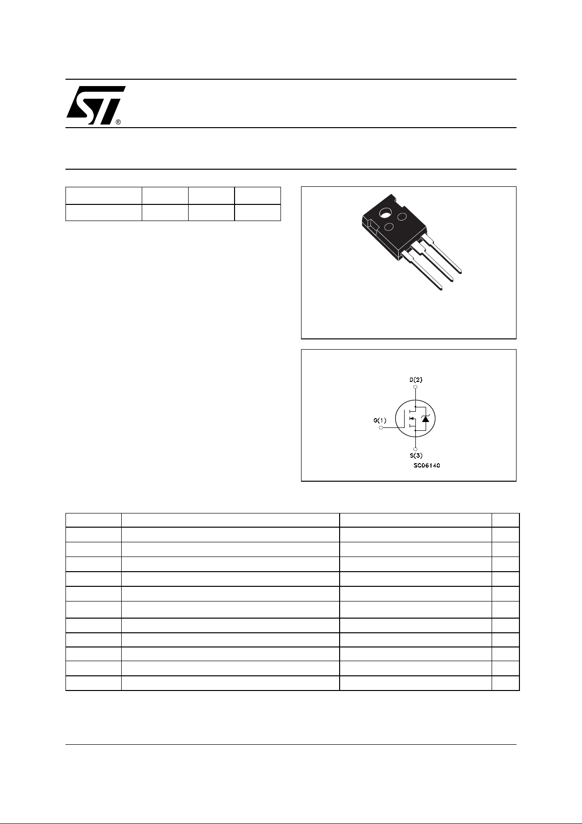
3
2
1
TO-247
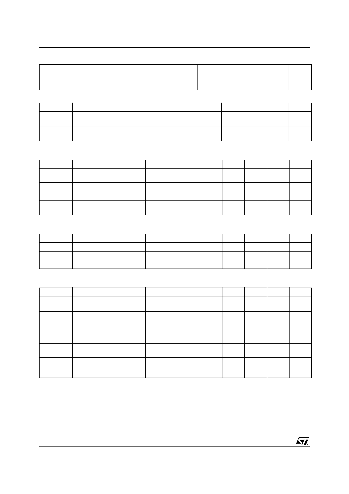
INTERNAL SCHEMATIC DIAGRAM
ABSOLUTE MAXIMUM RATINGS
Symbol Parameter Value Unit
V
DS
V
DGR
V
GS
I
D
I
D
I
DM
P
TOT
dv/dt Peak Diode Recovery voltage slope 6 V/ns
T
stg
T
j
(•)Pu l se width limited by safe operating area
(*)Limit ed only by maxi m um temperature allowed
August 2002
This is preliminary information on a new product now in development or undergoing evaluation. Details are subject to change without notice.
Drain-source Voltage (VGS = 0)
Drain-gate Voltage (RGS = 20 kΩ)
500 V
500 V
Gate- source Voltage ±30 V
Drain Current (continuous) at TC = 25°C
Drain Current (continuous) at TC = 100°C
(1)
Drain Current (pulsed) 56 A
Total Dissipation at TC = 25°C
14 A
8.8 A
175 W
Derating Factor 1.28 W/°C
Storage Temperature –65 to 150 °C
Max. Operating Junction Temperature 150 °C
(1)ISD ≤12A, di/dt ≤100A/µs, VDD ≤ V
(BR)DSS
, Tj ≤ T
JMAX.
1/5
STW14NM50
THERMA L D ATA
Rthj-case Thermal Resistance Junction-case Max 0.715 °C/W
Rthj-amb Thermal Resistance Junction-ambient Max 30 °C/W
T
l
AVALANCHE CHARACTERISTICS
Symbol Parameter Max Value Unit
I
AR
E
AS
Maximum Lead Temperature For Soldering Purpose 300 °C
Avalanche Current, Repetitive or Not-Repetitive
(pulse width limited by T
max)
j
Single Pulse Avalanche Energy
(starting T
= 25 °C, ID = IAR, VDD = 50 V)
j
12 A
400 mJ
ELECTRICAL CHARACTERISTICS (T
= 25 °C UNLESS OTHERWISE SPECIFIED)
CASE
OFF
Symbol Parameter Test Conditions Min. Typ. Max. Unit
Drain-source
Breakdown Voltage
Zero Gate Voltage
Drain Current (V
GS
Gate-body Leakage
Current (V
DS
= 0)
= 0)
= 250 µA, VGS = 0
I
D
= Max Rating
V
DS
V
= Max Rating, TC = 125 °C
DS
= ±30V
V
GS
500 V
1µA
10 µA
±100 nA
ON
V
(BR)DSS
I
DSS
I
GSS
(1)
Symbol Parameter Test Conditions Min. Typ. Max. Unit
V
V
GS(th)
R
DS(on)
Gate Threshold Voltage
Static Drain-source On
Resistance
= VGS, ID = 250µA
DS
= 10V, ID = 6A
V
GS
345V
0.3 0.35 Ω
DYNAMIC
Symbol Parameter Test Conditions Min. Typ. Max. Unit
V
> I
C
oss eq.
(1)
g
fs
C
iss
C
oss
C
rss
Forward Transconductance
Input Capacitance
Output Capacitance 180 pF
Reverse Transfer
Capacitance
(1) Equivalent Output
Capacitance
R
G
Gate Input Resistance
x R
D(on)
DS(on)max,
= 25V, f = 1 MHz, VGS = 0
I
DS
D
V
=6A
DS
VGS = 0V, VDS = 0V to 400V 90 pF
f=1 MHz Gate DC Bias = 0
Test Signal Level = 20mV
Open Drain
5.2 S
1000 pF
25 pF
1.6 Ω
2/5
1. C
is defined as a constant equivalent capacitance giving the same charging time as C
oss eq.
V
.
DSS
when VDS increase s fr om 0 to 80%
oss
 Loading...