

STW12NA50
N - CHANNEL ENHANCEMENT MODE
FAST POWER MOS TRANSISTOR
TYPE V
DSS
R
DS(on)
I
D
STW12NA50 500 V < 0.6 Ω 11.6 A
■ TYPICAL R
■ ± 30V GATE TO SOURCE VOLTAGE RATING
■ 100% AVALANCHE TESTED
■ REPETITIVE AVALANCHE DATA AT 100
■ LOW INTRINSIC CAPACITANCES
■ GATE GHARGE MINIMIZED
■ REDUCED THRESHOLD VOLTAGE SPREAD
DS(on)
= 0.5 Ω
o
C
DESCRIPTION
This series of POWER MOSFETS represents the
most advanced high voltage technology. The optimized cell layout coupled with a new proprietary
edge termination concur to give the device low
R
and gate charge, unequalled ruggedness
DS(on)
and superior switching performance.
APPLICATIONS
■ HIGH CURRENT, HIGH SPEED SWITCHING
■ SWITCH MODE POWERSUPPLIES (SMPS)
■ DC-AC CONVERTERS FOR WELDING
EQUIPMENT AND UNINTERRUPTIBLE
POWER SUPPLIES AND MOTOR DRIVE
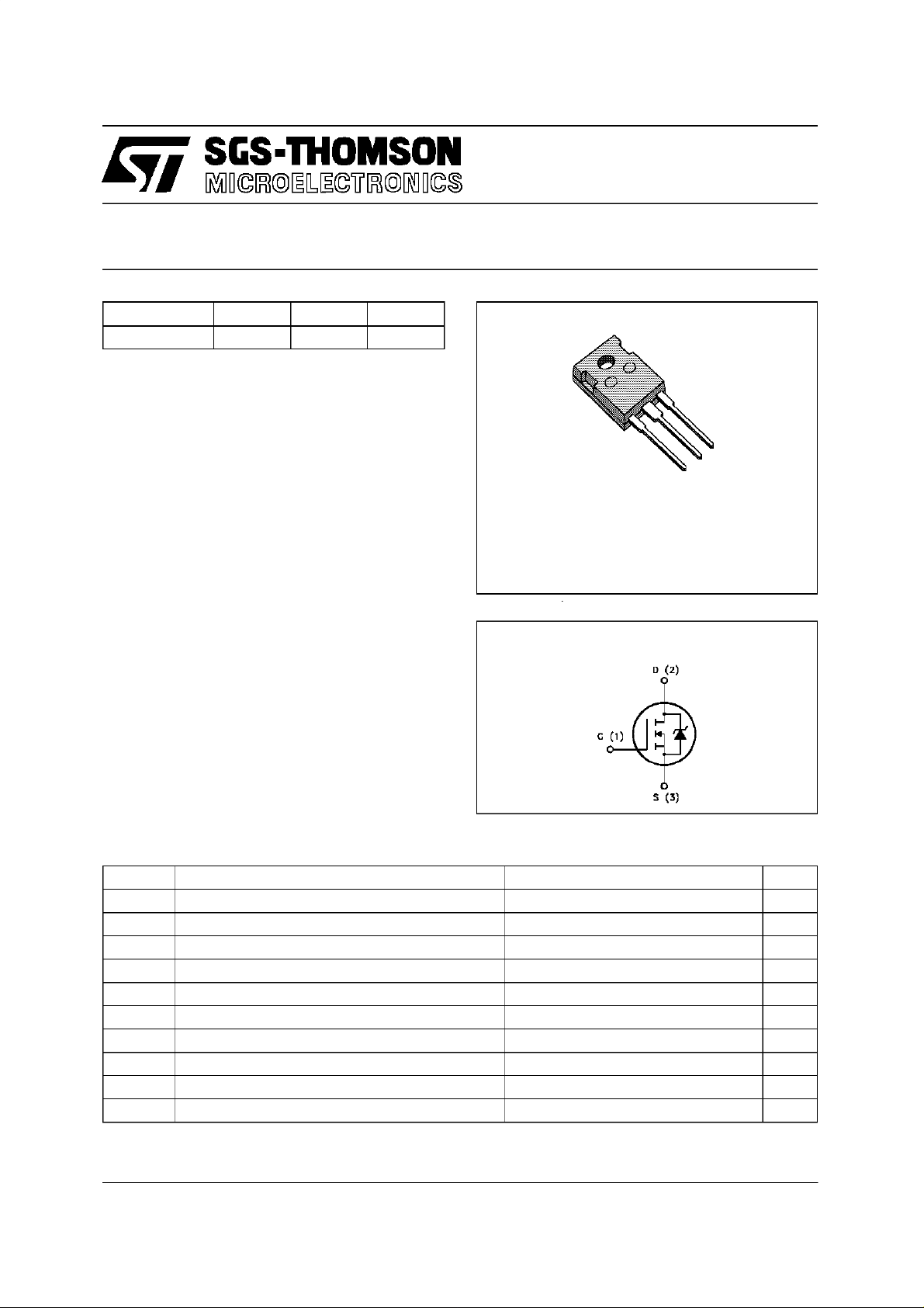
3
2
1
TO-247
INTERNAL SCHEMATIC DIAGRAM
ABSOLUTE MAXIMUM RATINGS
Symb o l Paramet er Val u e Unit
V
V
V
I
DM
P
T
(•) Pulsewidth limited bysafe operating area
December 1995
Drain - s ource Voltage (VGS= 0) 500 V
DS
Drain- gate Voltage (RGS=20kΩ) 500 V
DGR
Gate-source Voltage ± 30 V
GS
Drain Current (continuous) at Tc=25oC11.6A
I
D
Drain Current (continuous) at Tc=100oC7.3A
I
D
(•) Drain Current (pulsed) 46.4 A
Total Di ssipation a t Tc=25oC 170 W
tot
Derat ing Factor 1.36 W/
St or a ge Tem perature -65 t o 150
stg
Max. Operating Jun ction T emperature 150
T
j
o
C
o
C
o
C
1/9
STW12NA50
THERMAL DATA
R
thj-case
R
thj-amb
R
thj-amb
T
AVALANCHE CHARACTERISTICS
Symbol Parameter Max Valu e Uni t
I
AR
E
E
I
AR
Thermal Resistance Junction - cas e Max
Thermal Resistance Junction- ambient Max
Thermal Resistance Case-sink Typ
Maximum L ead Temperat ur e For Soldering Purpos e
l
Avalanc h e Cu rr ent , Repet itive or Not-Rep etitive
(pulse width limited by Tjmax, δ <1%)
Single Pul se Avalanche Ener gy
AS
(starti ng Tj=25oC, ID=IAR,VDD=50V)
Repetitive Avalanc he Energ y
AR
(pulse width limited by Tjmax, δ <1%)
Avalanc h e Cu rr ent , Repet itive or Not-Rep etitive
(Tc= 100oC, pulse width l imited by Tjmax, δ <1%)
0.73
30
0.1
300
11.6 A
670 mJ
26.5 mJ
7.3 A
o
C/W
o
C/W
o
C/W
o
C
ELECTRICAL CHARACTERISTICS (T
=25oC unless otherwisespecified)
case
OFF
Symbol Parameter Test Conditions Min. Typ. Max. Unit
V
(BR)DSS
Drain - s ource
ID=250µAVGS= 0 500 V
Break d own Volta ge
I
DSS
I
GSS
Zer o G at e V oltage
Drain Current (V
GS
Gat e- body Leakage
=0)
=MaxRating
V
DS
V
= Max Rating x 0.8 Tc=125oC
DS
25
250
VGS= ± 30 V ± 100 nA
Current (VDS=0)
ON (∗)
Symbol Parameter Test Conditions Min. Typ. Max. Unit
V
GS(th)
R
DS(on)
Gate Threshold Voltage VDS=VGSID=250µA 2.25 3 3.75 V
St at ic Drain-s our ce O n
VGS=10V ID=6A 0.5 0.6 Ω
Resistance
I
D(on)
On State Drain Current VDS>I
D(on)xRDS(on)max
12 A
VGS=10V
DYNAMIC
Symbol Parameter Test Conditions Min. Typ. Max. Unit
(∗)Forward
g
fs
Tr ansconductance
C
C
C
Input Capacitance
iss
Out put Capacitance
oss
Reverse Transfer
rss
Capacitance
VDS>I
D(on)xRDS(on)maxID
=6A 6 9 S
VDS=25V f=1MHz VGS= 0 1750
250
80
2500
370
130
µA
µA
pF
pF
pF
2/9
STW12NA50
ELECTRICAL CHARACTERISTICS (continued)
SWITCHING ON
Symbol Parameter Test Conditions Min. Typ. Max. Unit
t
d(on)
(di/dt)
Q
Q
Q
Turn-on T ime
t
Rise Time
r
Turn-on Current S lope VDD=400V ID=12A
on
Total Gate Charge
g
Gat e- Source Charge
gs
Gate-Drain Charge
gd
SWITCHING OFF
Symbol Parameter Test Conditions Min. Typ. Max. Unit
t
r(Voff)
t
Off -voltage Rise Time
t
Fall Time
f
Cross-over Time
c
SOURCE DRAINDIODE
VDD=250V ID=6A
RG=4.7 Ω VGS=10V
20
32
(see test circuit, figure 3)
190 A/µs
RG=47 Ω VGS=10V
(see test circuit, figure 5)
VDD= 400 V ID=12A VGS=10V 80
12
37
VDD=400V ID=12A
RG=4.7 Ω VGS=10V
(see test circuit, figure 5)
16
12
30
28
45
110 nC
22
18
42
ns
ns
nC
nC
ns
ns
ns
Symbol Parameter Test Conditions Min. Typ. Max. Unit
I
I
SDM
SD
Source-drain C urrent
(•)
Source-drain C urrent
11.6
46.4
(pulsed)
V
(∗) Forward On Voltage ISD=12A VGS=0 1.6 V
SD
t
Reverse Recovery
rr
Time
Q
Reverse Recovery
rr
ISD= 12 A di/dt = 100 A/µs
VDD= 100 V Tj=150oC
(see test circuit, figure 5)
600
10.2
Charge
I
RRM
Reverse Recovery
34
Current
(∗) Pulsed:Pulse duration = 300 µs, dutycycle 1.5 %
(•) Pulse widthlimited by safeoperating area
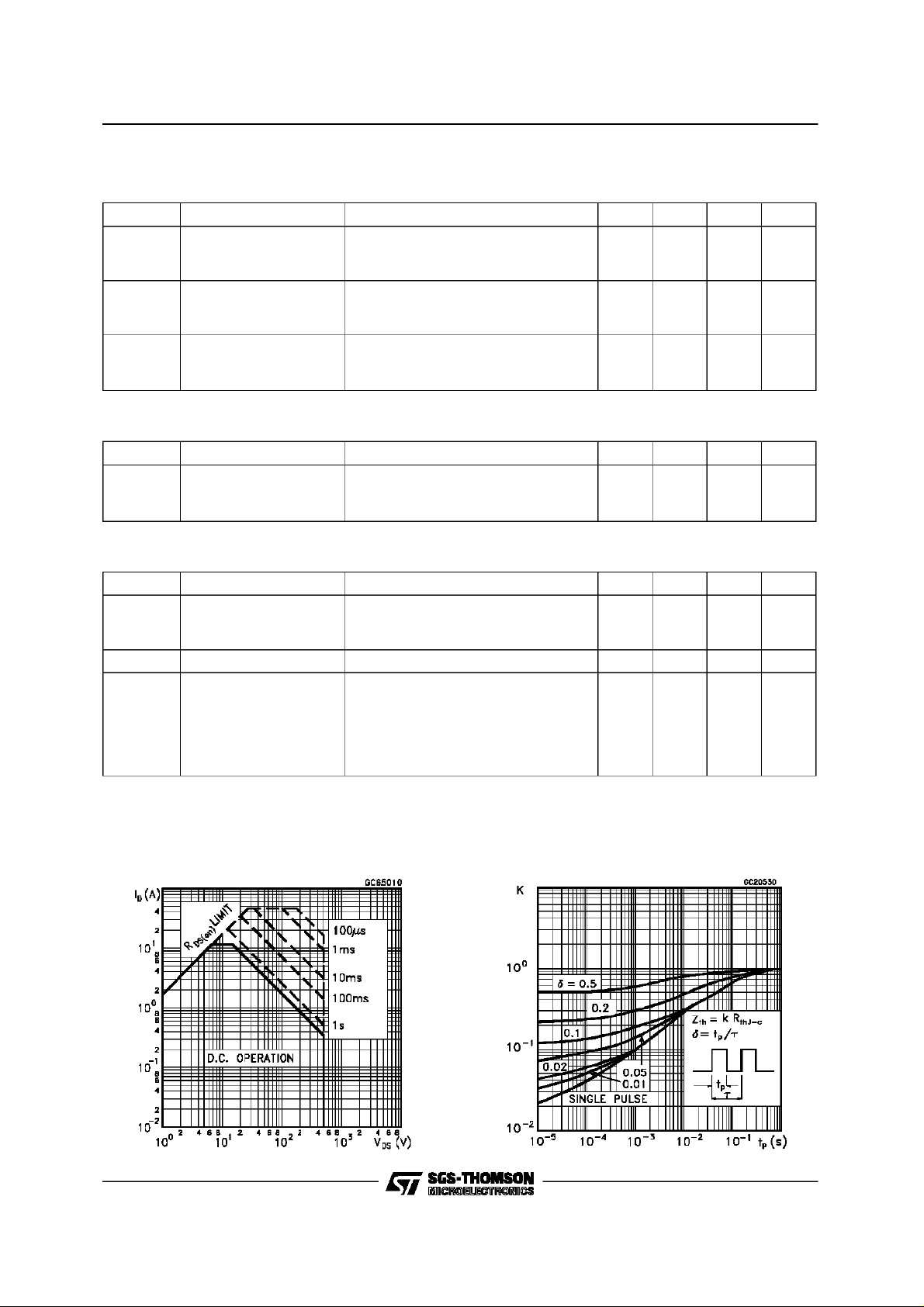
Safe Operating Areas Thermal Impedance
A
A
ns
µC
A
3/9
 Loading...