

SGS Thomson Microelectronics STW11NB80 Datasheet
STW11NB80
N-CHANNEL 800V - 0.65Ω - 11A - T0-247
PowerMESH MOSFET
TYPE V
DSS
R
DS(on)
I
D
ST W11NB 80 800 V < 0. 8 Ω 11 A
■ TYPICALR
■ EXTREMELY HIGH dv/dt CAPABILITY
■ ± 30VGATETO SOURCEVOLTAGERATING
■ 100%AVALANCHETESTED
■ VERYLOW INTRINSIC CAPACITANCES
■ GATECHARGE MINIMIZED
DS(on)
= 0.65 Ω
DESCRIPTION
Using the latesthigh voltage MESH OVERLAY
process, STMicroelectronics has designed an
advanced family of power MOSFETs with
outstanding performances. The new patent
pending strip layout coupled with the Company’s
proprietary edge termination structure, gives the
lowest RDS(on) per area, exceptional avalanche
and dv/dt capabilities and unrivalled gate charge
and switching characteristics.
APPLICATIONS
■ HIGHCURRENT, HIGH SPEED SWITCHING
■ SWITCHMODE POWER SUPPLIES(SMPS)
■ DC-AC CONVERTERS FORWELDING
EQUIPMENTAND UNINTERRUPTIBLE
POWERSUPPLIESAND MOTORDRIVE
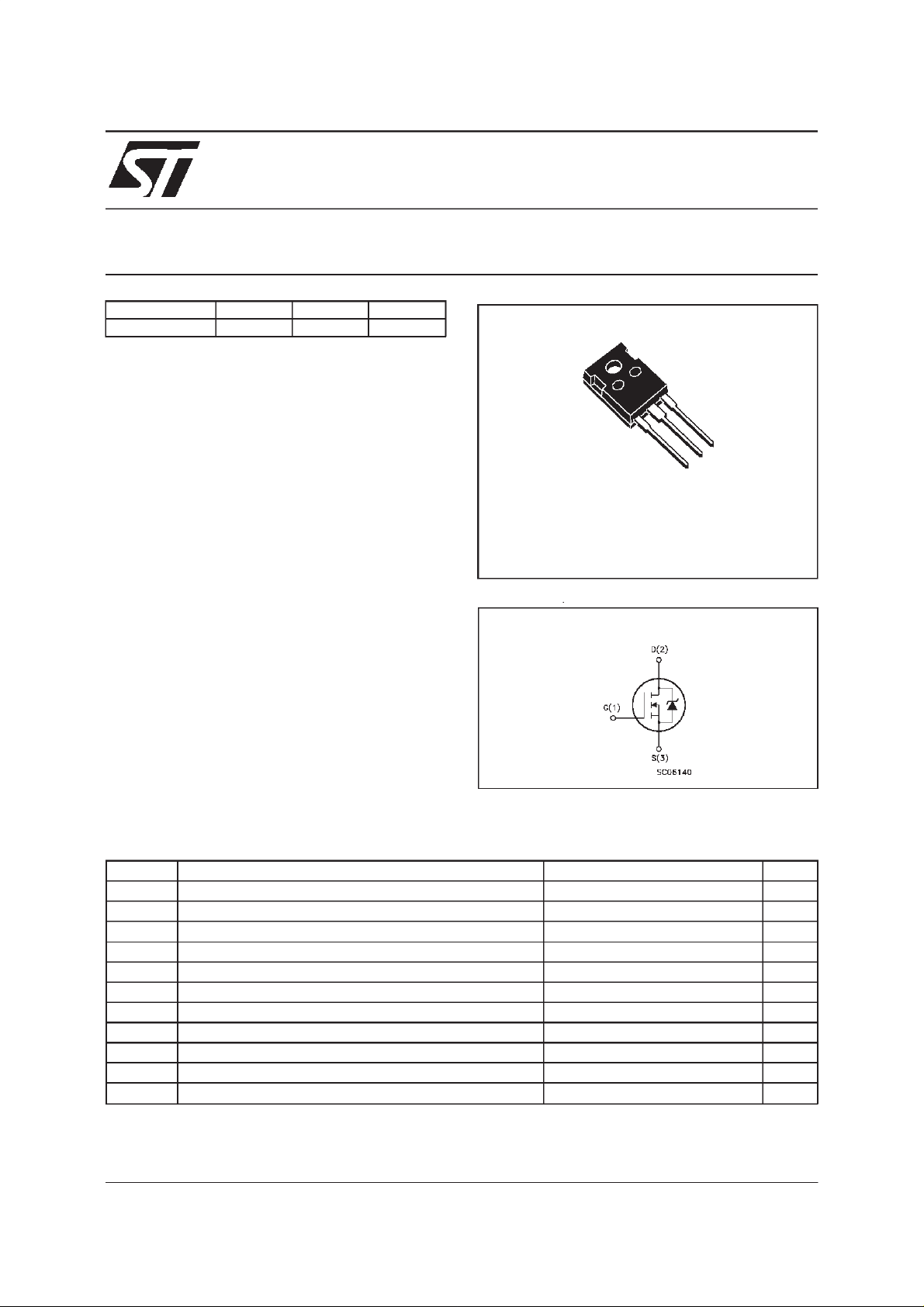
3
2
1
TO-247
INTERNAL SCHEMATIC DIAGRAM
ABSOLUTE MAXIMUM RATINGS
Symbol Parameter Value Unit
V
V
V
I
DM
P
dv/ dt(
T
(•) Pulse width limited by safeoperating area I
July 1999
Drain-source Voltage (VGS=0) 800 V
DS
Dra in- gate V oltage (RGS=20kΩ)
DGR
Gate -sourc e Volta ge
GS
Drain C urrent (co ntinuous) at Tc=25oC11A
I
D
Drain C urrent (co ntinuous) at Tc=100oC6.9A
I
D
800 V
30 V
±
(•) Drain C urrent (pu lsed) 44 A
Total Dissipation at Tc=25oC190W
tot
Derating Factor 1.52 W/
1) Peak Diode Rec ov e ry volt age slope 4 V/ns
St orage T e m pe rature -65 t o 150
stg
Max. Oper a t ing Junctio n T e mperatu r e 150
T
j
≤
11A, di/dt≤200A/µs, V
SD
≤
DD
V
(BR)DSS
,Tj≤T
JMAX
o
C
o
C
o
C
1/8
STW11NB80
THERMAL DATA
R
thj-case
R
thj-amb
R
thc-sink
T
AVALANCHE CHARACTERISTICS
Symbol Para meter Max Val ue Uni t
I
AR
E
Ther mal Resis t an ce Junc ti on-cas e Max 0.66
Ther mal Resis t an ce Junc ti on-ambien t Max
Thermal Resistance Case-sink Typ
Maximum Lead T emper at u re Fo r Solder ing Purp os e
l
Avalanche Current, Repet it ive or Not -Repet it ive
(pulse width limited by T
Single Pulse Avalanche Energy
AS
(starting T
=25oC, ID=IAR,VDD=50V)
j
max)
j
30
0.1
300
11 A
500 mJ
o
C/W
o
C/W
o
C/W
o
C
ELECTRICAL CHARACTERISTICS (T
=25oC unless otherwisespecified)
case
OFF
Symbol Parameter Test Conditions Min. Typ. Max. Unit
V
(BR)DSS
Drain-sourc e
=250µAVGS=0
I
D
800 V
Break d own Vo lt age
I
DSS
I
GSS
Zero Gate Voltage
Drain Cu rr ent ( V
GS
Gat e- b ody Leakage
Current (V
DS
=0)
=0)
V
=MaxRating
DS
= Max Rating Tc=125
V
DS
o
C
= ± 30 V
V
GS
1
50
± 100 nA
ON(∗)
Symbol Parameter Test Conditions Min. Typ. Max. Unit
V
GS(th)
Gate Threshold
V
DS=VGSID
= 250 µA
345V
Voltage
R
DS(on)
Static Drain-source O n
VGS=10V ID=5.5A 0.65 0.8 Ω
Resistanc e
I
D(on)
On S t ate Dra in Current VDS>I
D(on)xRDS(on)max
11 A
VGS=10V
DYNAMIC
Symbol Parameter Test Conditions Min. Typ. Max. Unit
g
(∗)Forward
fs
Tr ansconduc tance
C
C
C
Input Capac i t ance
iss
Out put Capac it a nc e
oss
Reverse Transfer
rss
Capacitance
VDS>I
D(on)xRDS(on)maxID
=5.5 A 10 S
VDS=25V f=1MHz VGS= 0 2900
350
33
µA
µ
Ω
pF
pF
pF
A
2/8
STW11NB80
ELECTRICAL CHARACTERISTICS
(continued)
SWITCHING ON
Symbol Parameter Test Conditions Min. Typ. Max. Unit
t
d(on)
Q
Q
Q
Turn-on Time
t
Rise Time
r
Total Gate Charge
g
Gat e- Source Charge
gs
Gate-Drain Charge
gd
VDD= 400 V ID=5A
=4.7 Ω VGS=10V
R
G
VDD= 640 V ID=10A VGS=10V
=4.7 Ω VGS=10V
R
G
30
13
70
18
31
SWITCHING OFF
Symbol Parameter Test Conditions Min. Typ. Max. Unit
t
r(Voff)
t
t
Off -voltage Rise Time
Fall Time
f
Cross-ov er Ti me
c
VDD= 640 V ID=10A
=4.7 Ω VGS=10V
R
G
26
23
37
SOURCEDRAINDIODE
Symbol Parameter Test Conditions Min. Typ. Max. Unit
I
SD
I
SDM
V
SD
t
Q
I
RRM
(∗) Pulsed: Pulse duration = 300 µs, duty cycle 1.5 %
(•) Pulse width limited by safe operating area
Source-drain Current
(•)
Source-drain Current
11
44
(pulsed)
(∗) Forwar d On V oltage ISD=11A VGS=0 1.6 V
Reverse Recov er y
rr
Time
Reverse Recov er y
rr
= 10 A di/dt = 100 A /µs
I
SD
= 100 V Tj=150oC
V
DD
900
9
Charge
Reverse Recov er y
20
Current
ns
ns
nC
nC
nC
ns
ns
ns
A
A
ns
µ
A
C
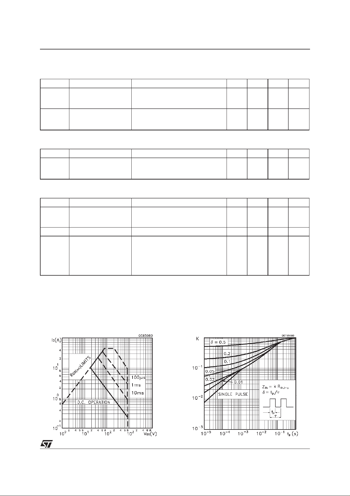
SafeOperating Area ThermalImpedance
3/8
 Loading...