

STV9432TAP
100MHz OSD FOR MONITOR INCLUDING
BEAM CURRENTS, VIDEO TIMING ANALYZER AND PWMs
■ MULTIFUNCTION OSD FOR MONITOR
■ INCLUDES FACILITIES FOR CUT-OFF VOLT-
AGE MONITORING:
- THREE 8 BITS ADC INPUTS
- ADC TRIGGER DURING RETRACE TIME OFA
PROGRAMMED LINE
■ INCLUDES FACILITIES FOR SCREEN SIZE &
CENTERING AUTO SETUP
- HS, VS, VIDEO TIMING MEASUREMENTS
■ 100MHz MAX. PIXEL CLOCK, AVAILABLE FOR
ANY LINE FREQUENCY BETWEEN 15 AND 140
kHz
■ 12 x 18 CHARACTER ROM FONT INCLUDES:
- 240 MONOCOLOR CHARACTERS
- 16 MULTICOLOR CHARACTERS
■ CHARACTER FLASHING
■ UP TO 1K CHARACTERS TEXT DISPLAY
■ ULTRAHIGH FREQUENCY PLL FOR
■ JITTER-FREE DISPLAY
■ FLEXIBLE DISPLAY:
- ANY CHARACTER WIDTH AND HEIGHT
- ANYWHERE IN THE SCREEN
■ SINGLE BYTE CHARACTER CODES AND
COLOR LOOK-UP TABLE FOR EASY PROGRAMMING AND FAST ACCESS
■ CHARACTER FLIP OPERATIONS
■ WIDE DISPLAY WINDOW ALLOWS PATTERN
GENERATION FORFACTORY ADJUSTMENTS
2
■ I
C BUS MCU INTERFACE
■ FIVE 8 BITS PWM DAC OUTPUTS
DESCRIPTION
Connected to a host MCU via its serial I2C Bus, the
STV9432TAP is a multifunction slave peripheral
device integrating the following blocks:
- On-screen Display. It includes a MASK PROGRAMMABLE ROM that holds the CUSTOM
CHARACTER FONT, a 1Kbytes RAM that stores
the code strings of the different lines of text to be
displayed, and a set of registers to program character sizes and colors. A built-in digital PLL, oper-
ating at very high frequency, gives an accurrate
display without visible jitter for a wide line frequency range from 15 to 140 kHz.
- Cut-off Monitoring Circuitry includes: 5 x 8 bits
PWM DACs, 3 x 8 bits ADCs and a programmable
ADC sampling trigger. It gives the possibility to
measure the three beam currents, during the horizontal flyback, at a given line in the frame, provided that the three ADC inputs are connected to a
beam current sensing circuitry. The values are
stored in three BEAM CURRENT REGISTERS,
and available for MCU read.
- Video Timing Analyzer. Using the HorizontalSync,
Vertical Sync, Horizontal Flyback, and ”Video
Active” inputs, a set of counters give the different
timing measurements necessary to analyze the
current Video timing characteristics in order to
make the automaticset-up of screen size and centering. The measurements are initialized on the
same programmable trigger line than in the above
cut-offmonitoring circuitry.
.
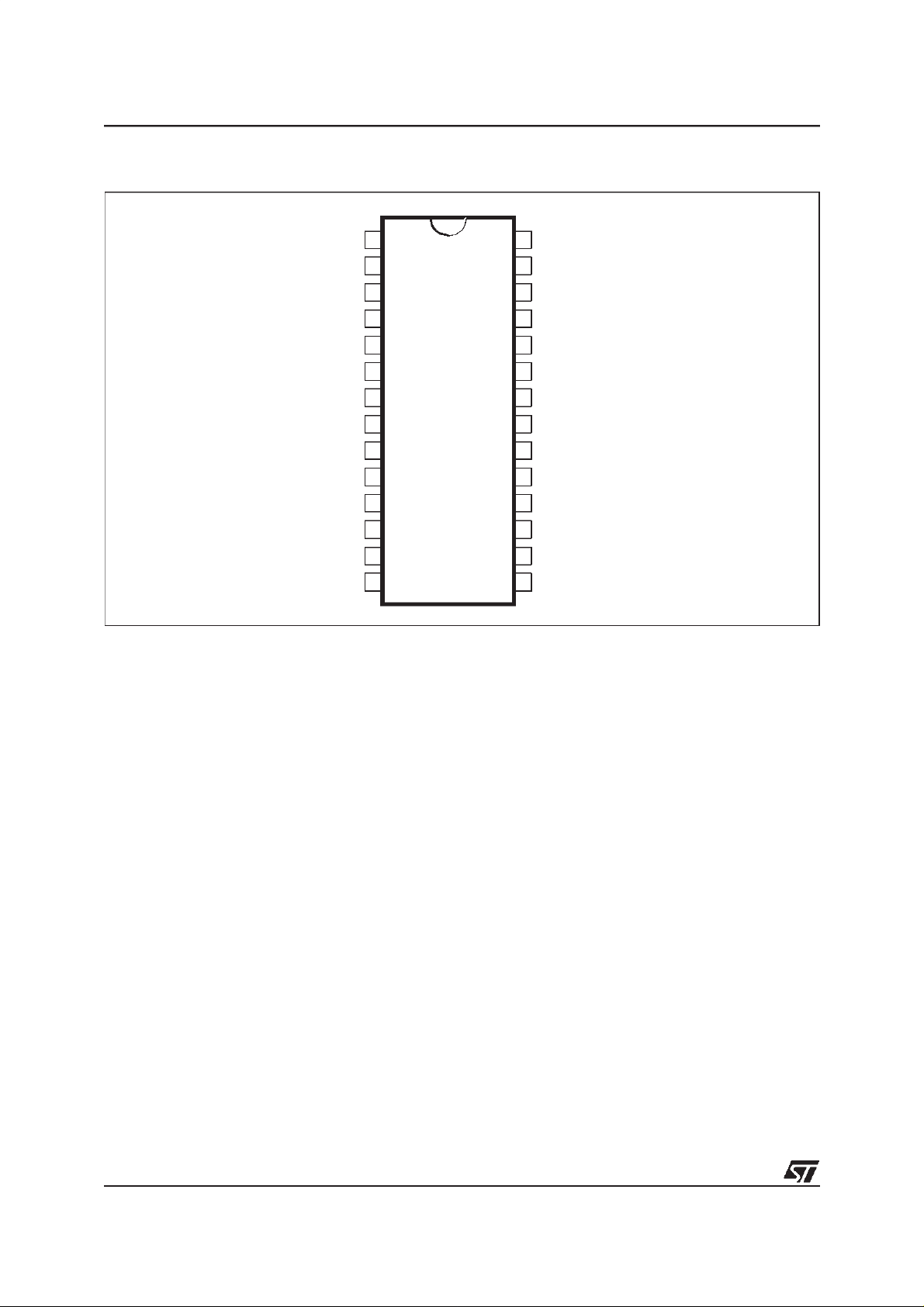
SO28
(Plastic Micropackage)
ORDER CODE:STV9432TAP
Version 4.0
February 2000 1/25
This ispreliminary information on a new product indevelopment orundergoing evaluation. Details are subject tochange without notice.
1
STV9432TAP
1 - PIN CONNECTIONS
FILTER
AGND
SDA
SCL
HFLY
DV
DVSS/OV
XTO
PWM1
PWM2
HS
VS
AV
XTI
1
2
3
4
5
6
7
8
9
DD
10
SS
11
12
13
14 PWM3
28
27
26
25
24
23
22
21
20
19
18
17
16
15
TEST
ADCREF
RCI
GCI
BCI
AV
DD
OV
DD
FBLK
BOUT
GOUT
ROUT
PWM5
PWM4
2/25
2
2 - PIN DESCRIPTION
Pin Number Symbol Type Description
1 FILTER I/O PLL Filter
2 AGND Power Analog Ground
3SDAI/O
4SCLI
5 HS I Horizontal Sync Input
6 VS I Vertical Sync Input
7 HFLY I Horizontal Flyback Input
8 AV I Active Video Input
9DV
10 DV
SS
DD
/OV
SS
Power Digital +5V Power Supply
Power Digital and RGB Output Ground
11 XTI I Crystal Oscillator Input
12 XTO O Crystal Oscillator Output
13 PWM1 O PWM DAC Output 1
14 PWM2 O PWM DAC Output 2
15 PWM3 O PWM DAC Output 3
16 PWM4 O PWM DAC Output 4
17 PWM5 O PWM DAC Output 5
18 ROUT O Red Output
19 GOUT O Green Output
20 BOUT O Blue Output
21 FBLK O Fast Blanking Output
22 OV
23 AV
DD
DD
Power +5V Supply for the RGB Outputs
Power Analog +5V Power Supply
24 BCI I Blue Beam Current Input
25 GCI I Green Beam Current Input
26 RCI I Red Beam Current Input
27 ADCREF I/O ADC Reference Voltage Pin
28 TEST I/O Pin to be connected to ground
2
C Bus Serial Data
I
2
C Bus Serial Clock
I
STV9432TAP
3/25
STV9432TAP
3 - BLOCK DIAGRAM
11
XTI
XTO
12
OSCILLATOR
8BITS
PWMs
13
14
15
16
17
PWM1
PWM2
PWM3
PWM4
PWM5
FILTER
HFLY
VS
HS
AV
RCI
GCI
BCI
ADCREF
AV
DD
DV
DD
5
26
25
24
27
23
1
7
6
8
PLL
TIMINGS
ANALYZER
BEAM
CURRENT
DISPLAY
CONTROLLER
1k BYTES RAM
CHARACTER
FONT ROM
22
18
19
20
21
10
2
OV
DD
ROUT
GOUT
BOUT
FBLK
DV
SS
AGND
/OV
SS
MEASURE-
MENT
2
C BUS
I
INTERFACE
3.3V
VOLTAGE REGULATOR
9
POWER-ON RESET
28
SDA
3
SCL
4
TEST
STV9432TAP
4 - ABSOLUTE MAXIMUM RATINGS
Symbol Parameter Value Unit
4/25
AV
DD
,DVDD,OV
V
IN
T
oper
T
stg
Supply Voltage -0.3, +6.0 V
DD
Input Voltage VSS-0.3, VDD+0.3 V
Operating Temperature 0, +70
Storage Temperature -40, +125
o
C
o
C
5 - ELECTRICAL CHARACTERISTICS
(VDD= 5V, VSS= 0V, GND =0V, TA=0to70o, unless otherwise specified)
Symbol Parameter Min. Typ. Max. Unit
SUPPLY
AVDD,DVDD,OV
+DIDD+OI
AI
DD
INPUTS (SCL, SDA)
V
IL
V
IH
I
IL
INPUTS (HS, VS, AV, HFLY)
V
IL
V
IH
V
HYST
I
PU
H
SIN
OUTPUTS (SDA open drain)
V
OL
OUTPUTS (R, G, B, FBLK)
V
OL
V
OH
OSCILLATOR (XTI, XTO)
I
IL
I
IH
V
IL
V
IH
V
OL
V
OH
ADCREF
V
REF
8 BITS PWM DACs 1,2,3,4,5
V
OL
V
OH
t
PWM
POWER-ON RESET
DV
DDTH
8 BITS ADC INPUTS (RCI, GCI, BCI)
V
IN
Z
IN
V
OFF
I
LEAK
ILE
DLE
Supply Voltage
DD
Analog and DigitalSupply Current
DD
Input Low Voltage
Input High Voltage
Input Leakage Current
Input Low Voltage
Input High Voltage HS, VS, AV
Schmidt Trigger Hysteresis
Pull-up Source Current (VIN= 0V)
Horinzontal Synchro Input Range
Output Low Voltage (IOL= 3mA)
Output Low Voltage (IOL= 3mA)
Output High Voltage (IOH= 3mA)
XTI Input Source Current (VIN= 0V)
XTI Input Sink Current (VIN=VDD)
XTI Input Low Voltage
XTI Input High Voltage
XTI Output Low Voltage (IOL= 3mA)
XTI Output High Voltage (IOH= 3mA)
Output Voltage Reference
Output Low Voltage (IOL= 1.6mA)
Output High Voltage (IOH= -0.8mA)
PWM Period
Supply Threshold Level
Input Voltage
Input Impedance
Input Offset Voltage
Input Leakage Current
Integral Linearity Error (Note 2)
Differential Linearity Error (Note 2)
HFLY
4.75 5 5.25 V
- - 150 mA
2.4 V
-1 +1 µA
2.4
3.6
15 - 140 kHz
00.4V
00.4V
0.8V
DD
315µA
315µA
0.7V
DD
00.4V
0.8V
DD
00.4V
VCC- 0.5 V
0V
-2 +2 LSB
-0.5 +0.5 LSB
STV9432TAP
0.8 V
0.8 V
V
0.4 V
100 µA
V
DD
1.4 V
V
DD
3.3 V
256 t
3.6 V
ADCREF
100 k
3LSB
050µA
V
V
V
OSC
V
Ω
5/25
STV9432TAP
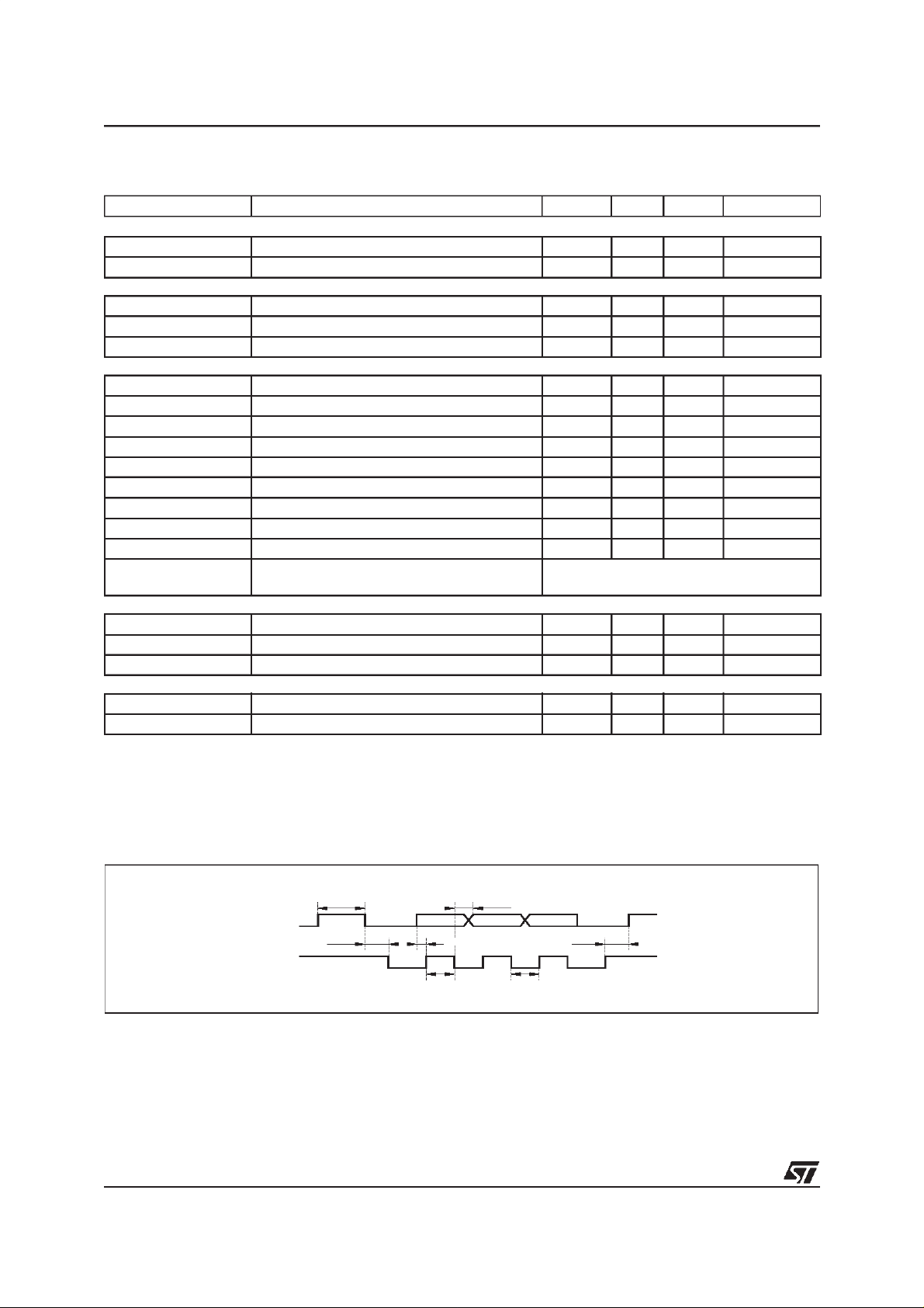
6 - TIMINGS
Symbol Parameter Min. Typ. Max. Unit
OSCILLATOR
f
OSC
f
PXL
R, G, B, FBLK (C
2
I
C INTERFACE: SDAAND SCL (see Figure 1)
t
ANALYZER (HS, HFLY,AV)
t
LOAD
t
R
t
F
t
SKEW
f
SCL
t
BUF
t
HDS
t
SUP
t
LOW
t
HIGH
t
HDAT
SUDAT
t
F
t
R
t
HLOW
HHIGH
Hs
ANALYZER (VS)
t
VLOW
t
VHIGH
Clock Frequency
Maximum PixelFrequency
= 30pF)
Rise Time (see Note 1)
Fall Time (see Note 1)
Skew between R, G, B, FBLK
SCL Clock Frequency
Time the bus must be free between 2 access
Hold Time for Start Condition
Set up Time for Stop Condition
The Low Period of Clock
The High Period of Clock
Hold Time Data
Set up Time Data
Fall Time of SDA
Rise Time of both SCL and SDA
Low Pulse Width(see Note 3)
High Pulse Width
Hs Frequency
Low Pulse Width
High Pulse Width
0 400 kHz
500 ns
500 ns
500 ns
400 ns
400 ns
0ns
500 ns
Depend on the pull-up resistor and the
2 4091 t
2 4091 t
2 4091 Lines
2 4091 Lines
Notes:
- These parameters are not tested on each unit. They are measured during our internal qualification procedure which
includes characterization on batches coming from corners of our processes and also temperature characterization.
- The ADC measurements are dependant on the noise. The test is done by correlation in order to screen out marginal
devices.
-t
HTIM
=3t
OSC
: 40.
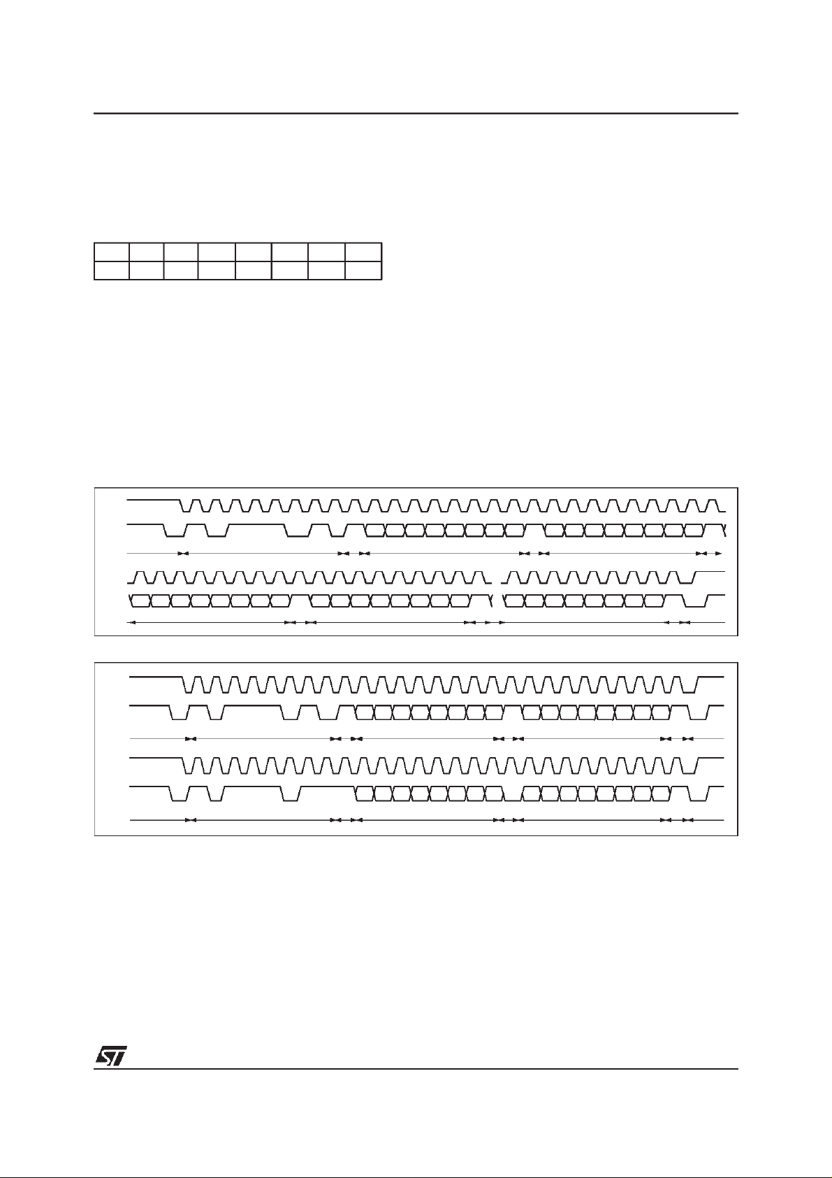
Figure 1.
8 MHz
100 MHz
5ns
5ns
5ns
20 ns
load capacitance
HTIM
HTIM
Hfly
6/25
STOP START DATA
t
BUF
SDA
t
HDS
SCL
t
HIGH
t
SUDAT
t
HDAT
t
LOW
t
SUP
STOP
7 - SERIAL INTERFACE
The 2-wires serial interface is an I2C interface. To be
connected to the I
address; the slave addressof the STV9432TAP is BA
(in hexadecimal).
A6 A5 A4 A3 A2 A1 A0 RW
1011101
7.1 - Data Transfer in Write Mode
The host MCU can write data into the STV9432TAP
registers or RAM.
To write data into the STV9432TAP, after a start, the
MCU must send (Figure2):
- First, the I
the R/W bit,
- The two bytes of the internal address where the
MCU wants to write data,
Figure 2. I2C Write Operation
SCL
SDA
2
C bus, a device must own its slave
2
C address slave byte with a lowlevel for
R/W
A7 A6 A5 A4 A3 A2 A1 A0 - - A13 A12 A11 A10 A9 A8
I2C Slave Address
ACK LSB Address ACK MSB Address ACKStart
STV9432TAP
- The successivebytes of data.
All bytes are sent MSB bit first and the write data
transfer is closed by a stop.
7.2 - Data Transfer in ReadMode
The host MCU can read data from the STV9432TAP
register, RAM or ROM.
To read data from the STV9432TAP (Figure 3), the
MCU must send 2 different I
one is made of I
2
C slave address byte with R/W bit at
low level and the 2 internal address bytes.
The second one is made of I
with R/W bit at high level and all the successive data
bytes read at successive addresses starting from the
initial address given by the first sequence.
2
C sequences. The first
2
C slave address byte
SCL
D7 D6 D5 D4 D3 D2 D1 D0 D7 D6 D5 D4 D3 D2 D1 D0 D7 D6 D5 D4 D3 D2 D1 D0
SDA
Figure 3. I2C Read Operation
SCL
SDA
2
I
C SlaveAddress
SCL
SDA R/W
I2C SlaveAddress
ACK ACKDataByte 1 DataByte2 ACK DataByte n Stop
R/W
A7 A6 A5 A4 A3 A2 A1 A0
ACK LSB Address ACK MSB Address ACKStart
D7 D6 D5 D4 D3 D2 D1 D0
*
ACK ACK DataByte n ACKStart
Data Byte1
- - A13 A12
D7 D6 D5 D4 D3 D2 D1 D0
A10 A10 A9 A8
Stop
Stop
7/25
STV9432TAP
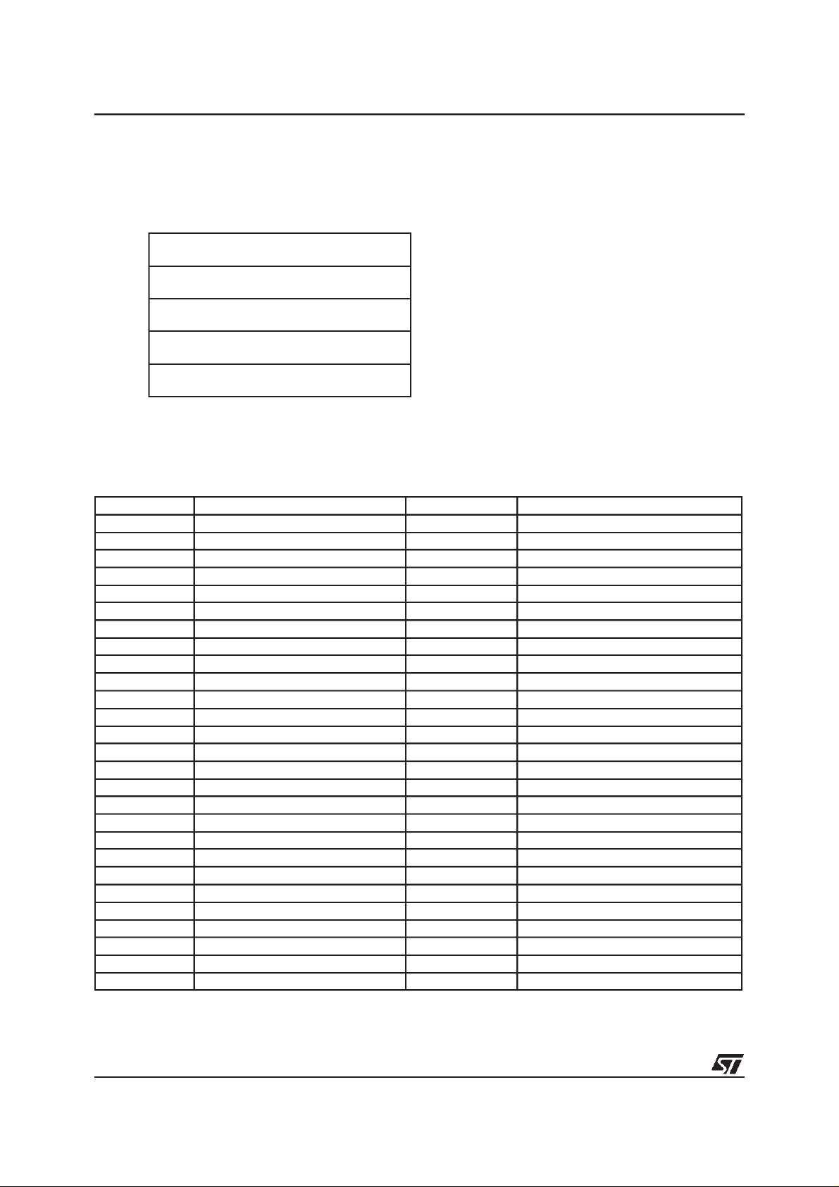
7.3 - ADDRESSING SPACE
7.3.1 - General Mapping
STV9432TAP registers, RAM and ROM are mapped in a 32Kbytes addressing space.
The mapping is the following:
0000
03FF
0400
07FF
0800
3FFF
4000
403F
4040
7FFF
1024 bytes RAM
Empty Space
Character Generator ROM
Internal Registers
Empty Space
Descriptors and character codes
Important Notice:
All 16 bits datas are mapped LSB byte at lower address and MSB byte at higher address.
- Example: H1 12 bits register: @4000: 8 LSB bits - @4001: 4 MSB bits.
- Descriptors must also be written to RAM LSB byte first.
7.3.2 - I2C Registers Mapping
4000 H1 LSB 4024 Color 4
4001 H1 MSB 4025 Color 5
4002 H2 LSB 4026 Color 6
4003 H2 MSB 4027 Color 7
4004 H3 LSB 4028 Color 8
4005 H3 MSB 4029 Color 9
4006 H4 LSB 402A Color 10
4007 H4 MSB 402B Color 11
4008 H5 LSB 402C Color 12
4009 H5 MSB 402D Color 13
400A H6 LSB 402E Color 14
400B H6 MSB 402F Color 15
400C V1 LSB 4030 Line Duration
400D V1 MSB 4031 Top Margin
400E V2 LSB 4032 Horizontal Delay
400F V2 MSB 4033 Character Height
4010 V3 LSB 4034 Display Control
4011 V3 MSB 4035 Locking Time Constant
4012 RCI 4036 Capture Time Constant
4013 GCI 4037 Initial Pixel Period
4014 BCI 4038 PWM1
4015 SBN 4039 PWM2
4016 TIMG 403A PWM3
4017-401F Reserved 403B PWM4
4020 Color 0 403C PWM5
4021 Color 1 403D-403E Reserved
4022 Color 2 403F RST
4023 Color 3 4040-7FFF Reserved
8/25
 Loading...