


SGS Thomson Microelectronics STV9429, STV9427, STV9428 Datasheet
MULTISYNCH ON-SCREEN DISPLAY FOR MONITOR
.
CMOS SINGLE CHIP OSD FOR MONIT OR
.
BUILT IN 1 KBYTE RAM HOLDING :
- CHARACTER CODES
- USER DEFINABLE CHARACTERS
.
207 ALPHANUMERIC CHARACTERS OR
GRAPHIC SYMBOLS IN INTERNAL ROM
.
12 x 18 CHARACTER DOT MATRIX
.
PROGRAMMABLE ACCENTUA TED CHARACTER SET
.
CHARACTER BLINKING
.
RAM DEFINABLE COLOR LOOK UP TABLE
.
UP TO 16 USER DEFINABLE CHA RACTE RS
.
UP TO 80MHz PIXEL CLOCK
.
INTERNAL HORIZONTAL PLL (15 TO 120kHz )
.
PROGRAMMABLE VERTICAL HEIGHT OF
CHARACTER WITH A SLICE INTERPOLATOR
TO MEET MULTI-SYNCH REQUIREMENTS
.
PROGRAMMABLE VERTICAL AND HORIZONTAL POSITIONING
.
FLEXIBLE SCREEN DESCRI PT ION
.
22 CONTROL CODES FOR POWERFULL
SERIAL ATTRIBUTES
.
2-WIRES ASYNCHRONOUS SERIAL MCU
INTERFACE (I
.
8 x 8 BITS PWM DAC OUTPUTS
.
SINGL E PO SITIVE 5V SUPPLY
2
C PROTOCOL)
STV9427
STV9428-STV9429
HIGH SPEED
8 x 8 bits PWM DAC are available to provide DC
voltage control to other peripherals.
The STV9427/28/29 provides the user an easy to
use and cost effective solution to display alphanumeric or graphic information on monitor screen.
DIP16
(Plastic Package)
ORDER CODE :
(Plastic Package)
STV9427
DIP20
DESCRIPTION
The STV9427/28/29 is an ON SCREEN DISPLAY
for monitor. It is built as a slave peripheral connected to a host MCU via a serial I
includes a display memory, controls all the display
attributes and generates pixels from the data read
in its on chip memory. The line PLL and a special
slice interpolator allow to have a display aspect
which does not depend on the line and frame
frequencies. I
transparent internal access to prepare the next
pages during the display of the current page. Toggle from one page to another by programming only
one register.
June 1998
2
C interface allows MCU to make
2
C bus. It
ORDER CODE : STV9428
DIP24
(Plastic Package)
ORDER CODE :
STV9429
1/20
STV9427 - STV9428 - STV9429
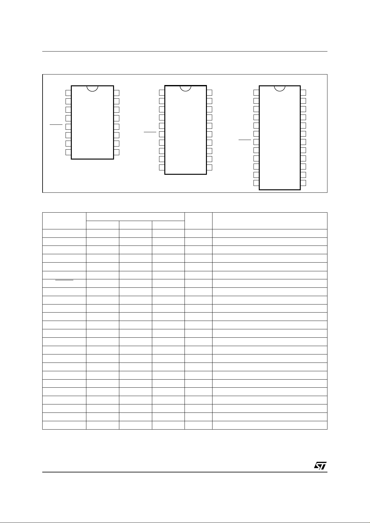
PIN CONNECTIONS
V
DD1
TST
XTO
XTI
RESET
VSYNC
HSYNC
GND
DIP16 (STV9427)
1
2
3
4
5
6
7
8
16
15
14
13
12
11
10
V
DD2
B
G
R
FBLK
GND
SDA
SCL
9
PWM1
RESET
VSYNC
HSYNC
PWM2
DIP20 (STV9428)
1
2
V
DD1
3
TST
XTI
4
5
6
7
8
9
10
XTO
GND
20
PWM0
19
V
DD2
18
B
17
G
16
R
15
FBLK
14
GND
13
SDA
12
SCL
11
PWM3
PWM6
PWM1
V
DD1
TST
XTO
XTI
RESET
VSYNC
HSYNC
GND
PWM2
PIN DESCRIPTION
Symbol
DIP24 DIP20 DIP16
PWM6 1 - - O DAC0 Output
PWM1 2 1 - O DAC1 Output
V
DD1
3 2 1 S +5V Logic Supply
TST 4 3 2 I Reserved (not to be connected)
XTO 5 4 3 O Crystal Output
XTI 6 5 4 I Crystal or Clock Input
RESET 7 6 5 I Reset Input (Active Low)
VSYNC 8 7 6 I Vertical Sync Input
HSYNC 9 8 7 I Horizontal Sync Input
GND 10 9 8 S Logic Ground
PWM2 11 10 - O DAC2 Output
PWM5 12 - - O DAC3 Output
PWM4 13 - - O DAC4 Output
PWM3 14 11 - O DAC5 Output
SCL 15 12 9 I Serial Clock
SDA 16 13 10 I/O Serial Input/output Data
GND 17 14 11 S Ground
FBLK 18 15 12 O Fast Blanking Output
R 19 16 13 O Red Output
G 20 17 14 O Green Output
B 21 18 15 O Blue Output
V
DD2
22 19 16 S +5V Outputs Supply
PWM0 23 20 - O DAC6 Output
PWM7 24 - - O DAC7 Output
Pin Number
I/O Description
DIP24 (STV9429)
1
2
3
4
5
6
7
8
9
10
11
12
24
23
22
21
20
19
18
17
16
15
14
13
PWM7
PWM0
V
DD2
B
G
R
FBLK
GND
SDA
SCL
PWM3
PWM4PWM5
9427-01.TBL 9427-01.EPS / 9428-01.EPS / 9 429-01.EPS
2/20
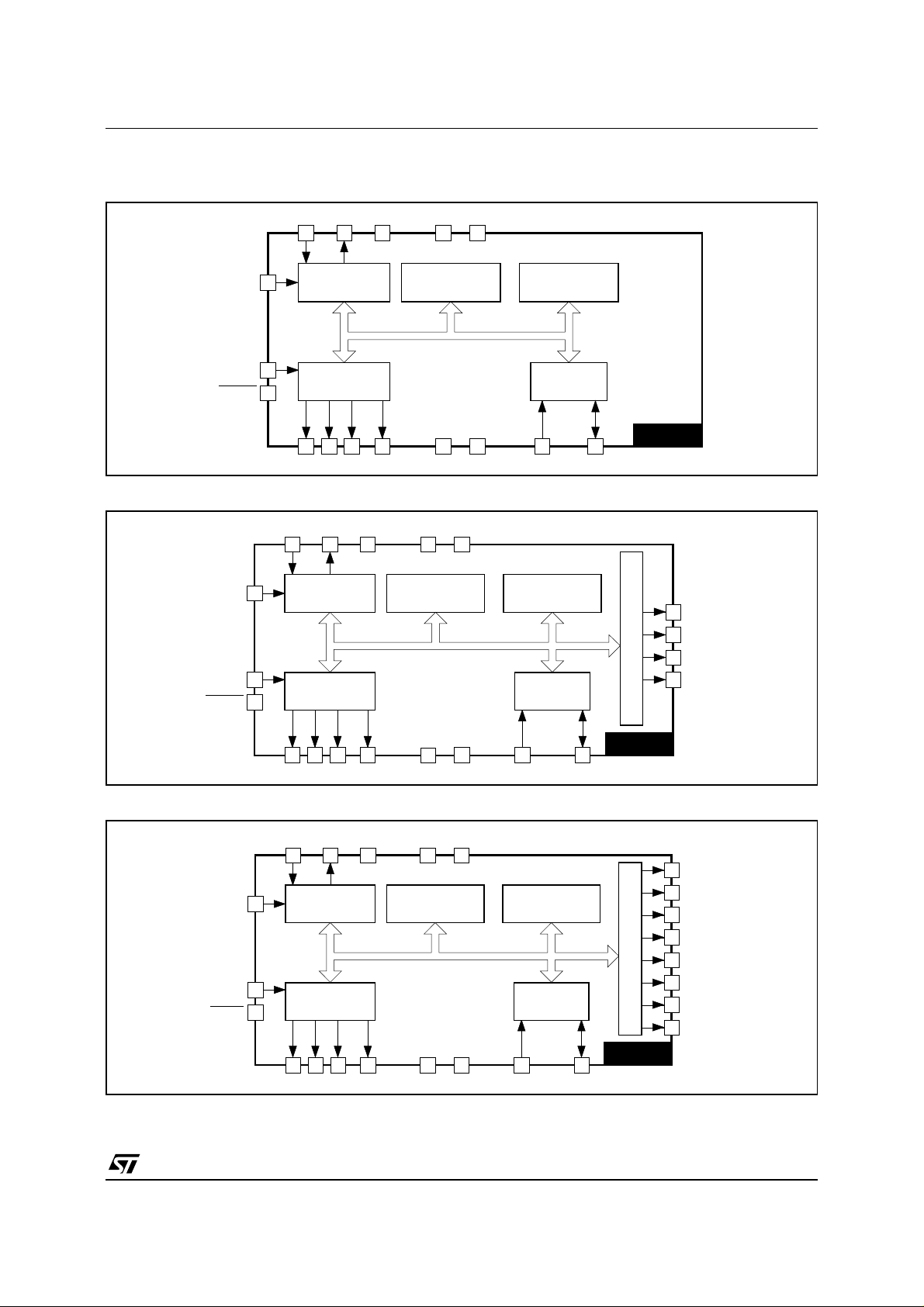
BLOCK DIAGRAMS
STV9427
XTI XTO
TST V
234
V
DD1
1
STV9427 - STV9428 - STV9429
DD2
16
STV9428
HSYNC
VSYNC
RESET
HSYNC
VSYNC
RESET
7
6
5
XTI XTO TST
5 4 3
HORIZONTAL
8
DIGITAL PLL
7
CONTROLLER
6
HORIZONTAL
DIGITAL PLL
4K ROM
1K RAM
Address/Data
DISPLAY
CONTROLLER
12
RGBFBLK GND SCL
V
2
4K ROM
Address/Data
DISPLAY
GND
DD1
1113 14 15
8
V
DD2
19
2
I C BUS
INTERFACE
9 10
1K RAM
I2C BUS
INTERFACE
SDA
STV9427
20
11
PWM
10
1
9427-02.EPS
PWM0
PWM3
PWM2
PWM1
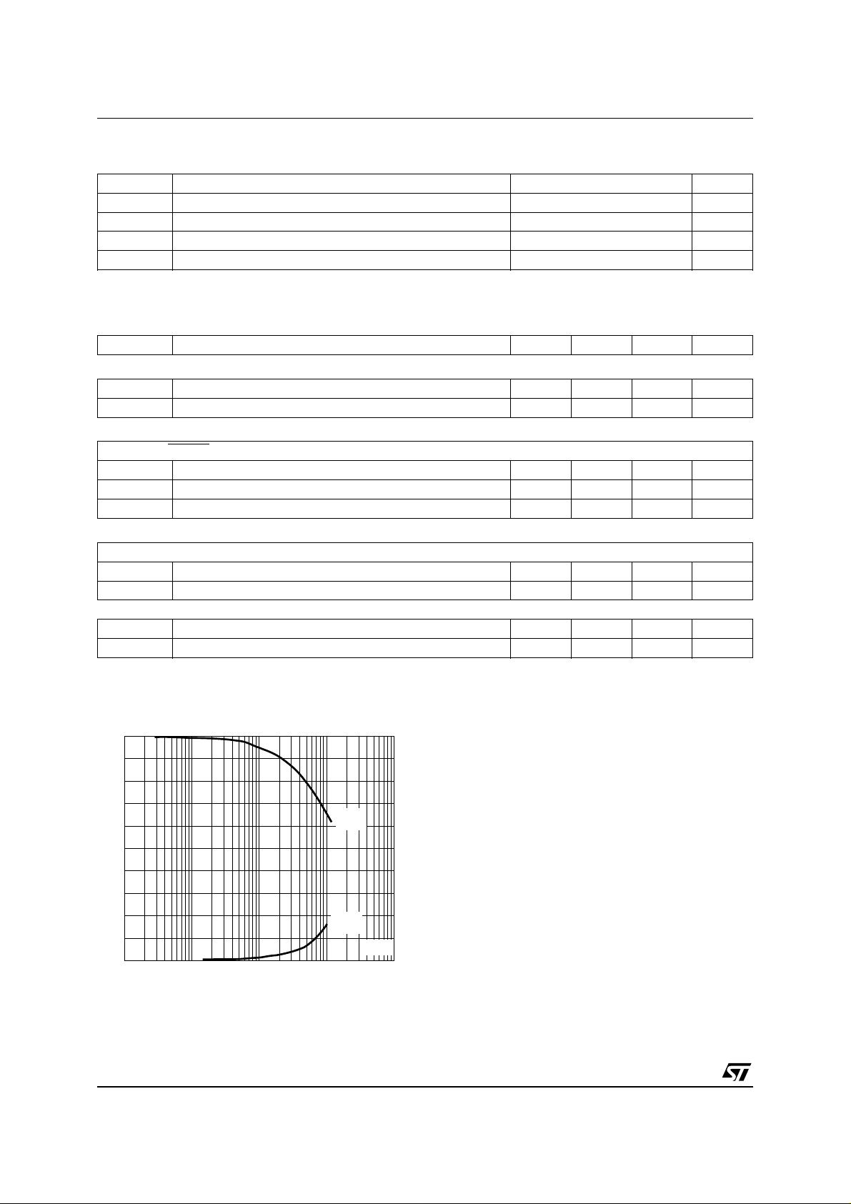
STV9429
HSYNC
VSYNC
RESET
16 17 18 15 14 12 13
RGBFBLK GND SCL SDA
XTI XTO TST
6 5 4
HORIZONTAL
9
DIGITAL PLL
Address/Data
8
7
DISPLAY
CONTROLLER
19 20 21 18 17 15 16
RGBFBLK GND SCL SDA
9
GND
V
DD1
3
4K ROM
10
GND
V
DD2
22
INTERFACE
1K RAM
I2C BUS
STV9428
PWM
STV9429
24
23
14
13
12
11
2
1
9428-02.EPS
PWM7
PWM0
PWM3
PWM4
PWM5
PWM2
PWM1
PWM6
9429-02.EPS
3/20
STV9427 - STV9428 - STV9429
ABSOLUTE MAXIMUM RATINGS
Symbol Parameter Value Unit
V
DD
V
IN
T
OPER
T
STG
ELECTRICAL CHARACTERI STICS
= V
(V
DD1
Symbol Parameter Min. Typ. Max. Unit
SUPPLY
V
DD
I
DD
INPUTS
SCL, SDA, RESET, VSYNC and HSYNC
V
IL
V
IH
I
IL
OUTPUTS
SDA open drain and PWMi (i = 0 to 7)
V
OL
V
OH
R, G, B, FBLK
V
OL
V
OH
Supply Voltage -0.3, +7.0 V
Input Voltage -0.3, +7.0 V
Operating Temperature 0, +70 °C
Storage Temperature -40, +125 °C
= 5V, VSS = 0V, TA = 0 to 70°C, f
DD2
= 8 to 15MHz, TEST = 0 V, unless otherwise s p ec ified)
XTAL
Supply Voltage 4.75 5 5.25 V
Supply Current - 65 90 mA
Input Low Voltage 0.8 V
Input High Voltage 2.4 V
Input Leakage Current -10 +10 µA
Output Low Voltage (IOL = 1.6mA) 0 0.4 V
Output High Voltage (IOH = -0.1mA) 0.9V
DD
V
DD
Output Low Voltage (IOL = 1.6mA) 0 0.4 V
Output High Voltage (IOH = -0.1mA) 0.9V
DD
V
DD
9427-02.TBL
V
V
9427-03.TBL
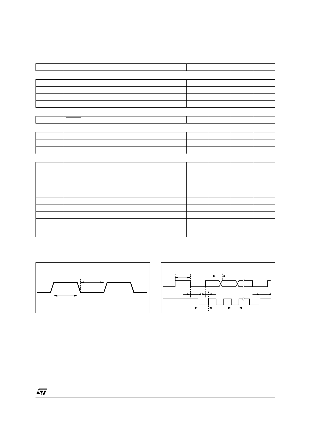
Figure 1 :
V
OL OH
5
2.5
0
-5
10
4/20
R, G, B, FBLK Typical Outputs Static
Characteristics
(V)
V
,
V
OH
V
OL
I (A)
10
-4
10
-3
10
-2
10
-1
9427-17.EPS
STV9427 - STV9428 - STV9429
TIMINGS
Symbol Parameter Min. Typ. Max. Unit
OSCILATOR INPUT : XTI (see Figure 2)
t
WH
t
WL
f
XTAL
f
PXL
RESET
t
RES
R, G, B, FBLK (C
t
R
t
F
t
SKEW
2
C INTERFACE : SDA AND SCL (see Figure 3)
I
f
SCL
t
BUF
t
HDS
t
SUP
t
LOW
t
HIGH
t
HDAT
t
SUDAT
t
F
t
R
Note 1 :
Clock High Level 20 ns
Clock Low Level 20 ns
Clock Frequency 6 15 MHz
Pixel Frequency 30 80 MHz
RESET Low Level Pulse 4 µs
= 30pF)
LOAD
Rise Time (see Note 1) 5 ns
Fall Time (see Note 1) 5 ns
Skew between R, G, B, FBLK 5 ns
SCL Clock Frequency (Horizontal frequency = 32kHz) 288 kHz
Time the bus must be free between 2 access 500 ns
Hold Time for Start Condition 500 ns
Set up Time for Stop Condition 500 ns
Clock Low Level 400 ns
Clock High Level 400 ns
Hold Time Data 0 ns
Set up Time Data 500 ns
SDA Fall Time 20 ns
SCL and SDA Rise Time
These parameters are not tested on each unit. They are measured during our internal qualification procedure whic h i ncludes
characterization on batches comming from corners of our processes and also temperature characterization.
Depend on the pull-up resistor
and on the load capacitance
9427-04.TBL
Figure 2
XTI
Figure 3
Stop Start Data Stop
t
t
BUF
HDS
t
WL
t
WH
SDA
SCL
t
9427-03.EPS
HIGH
t
SUDAT
t
HDAT
t
SUP
t
LOW
9427-04.EPS
5/20
STV9427 - STV9428 - STV9429
FUNCTIONAL DESCRIPTION
The STV9427/28/29 display processor operation is
controlled by a host MCU via the I
fully programmable through internal read/write registers and performs all the display functions by
generating pixels from data stored in its internal
memory. After the page downloading from the
MCU, the STV9427/28 /29 refreshes screen by
its built in p rocessor, without a ny MCU control
(access). In addition, the host MCU has a direct
access to the on c hip 1Kbytes RAM du ring the
display of the curr ent page to make any update
of its c ontents.
With the STV9427/28/29, a page displayed on the
screen is made of several strips which can be of 2
types : spacing or character and which are described by a table of descriptors and character
codes in RAM. Several pages can be downloaded
at the same time in the RAM and the choice of the
current display page is made by programming the
DISPLAY CONTROL register.
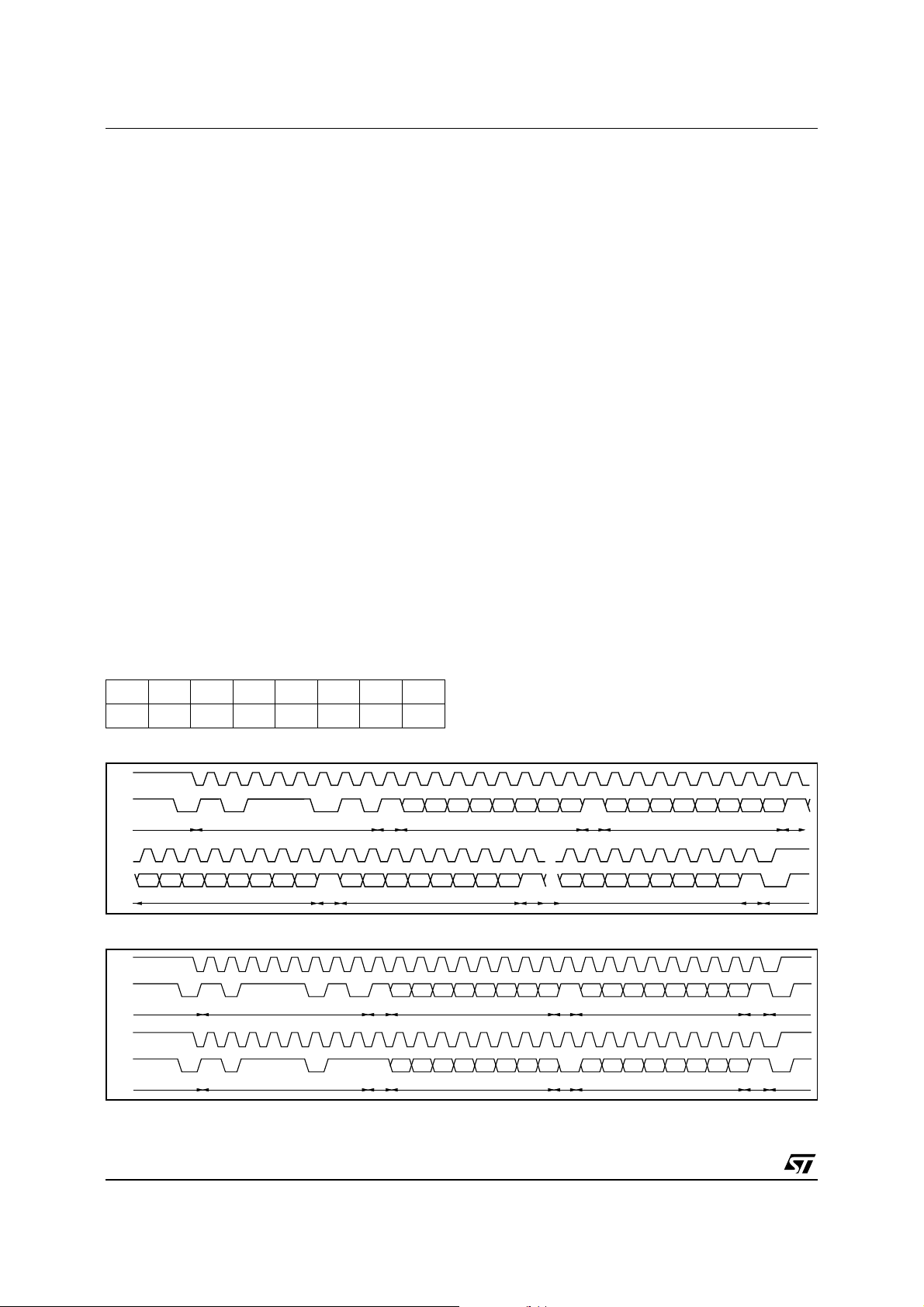
I - Serial Interface
The 2-wires serial interface is an I
be connected to the I
2
C bus, a device must own its
slave address ; the slave address of the
STV9427/28/29 is BA (in hexadecimal).
A6 A5 A4 A3 A2 A1 A0 R/W
1011101
2
Figure 4 :
MCU I
C Write Operation
2
C interface. It is
2
C interface. To
I.1 - Data Transfer in Write Mode
The host MCU can write data into the
STV9427/28/29 registers or RAM.
T o write data into the STV9427/28/29, after a start,
the MCU must send (Figure 4) :
- First, the I
2
C address slave byte with a low level
for the R/W bit,
- The two bytes of the internal address where the
MCU wants to write data(s),
- The successive bytes of data(s).
All bytes are sent MSB bit first and the write data
transfer is closed by a stop.
Each byte is synchronously transfered at each
HSYNC period.
I.2 - Data Transfer in Read Mode
The host MCU can read data from the
STV9427/28/29 registers, RAM or ROM.
To read data fr om the STV9427/28/29 (Figure 5),
the MCU must send 2 different I
first one is made of I
2
C slave address byte with R/W
bit at low level and the 2 internal address bytes.
The second one is made of I
2
C sequences. The
2
C slave address byte
with R/W bit at high le vel and all the successive
data bytes read at successive addresses starting
from the initial address given by the first sequence.
Each byte is synchronously transfered at each
HSYNC period. The first data byte, in read mode,
is available one Hsync period after the acknowledge of the address byte.
SCL
R/W
SDA
I2C Slave Address
SCL
D7 D6 D5 D4 D3 D2 D1 D0 D7 D6 D5 D4 D3 D2 D1 D0 D7 D6 D5 D4 D3 D2 D1 D0
SDA
ACK ACKData Byte 1 Data Byte 2 ACK Data Byte n Stop
2
Figure 5 :
SCL
SDA
SCL
SDA
Note :
MCU I
Start
Start
The first data bit out (D7) is valid after one scanline period.
C Read Operation
R/W
I2C Slave Address
R/W
I2C Slave Address
A7 A6 A5 A4 A3 A2 A1 A0 - - A13 A12 A11 A10 A9 A8
ACK LSB Address ACK MSB Address ACKStart
A7 A6 A5 A4 A3 A2 A1
ACK
D7 D6 D5 D4 D3 D2 D1 D0
*
ACK
LSB Address ACK
Data Byte 1
A0
--
A13 A12
MSB Address
D7 D6 D5 D4 D3 D2 D1 D0
ACK
Data Byte n
6/20
A10
A10
9427-05.EPS
A9
A8
ACK
Stop
ACK
Stop
9427-06.EPS