CRT AND LCD SEMI-GRAPHIC DISPLAY PROCESSOR
.
CMOS SINGLE CHIP CRT AND LCD DISPLAYPROCESSOR
.
BUILTIN6 KBYTERAM
.
25 ROWSOR MOREOF40 CHARACTERS
.
CRTMODE :
- ANALOGY LUMINANCE OUTPUT OF 4BIT DAC
- R,G,BDIGITALCOLOROUTPUTS
- FAST BLANKING OUTPUT FOR VIDEO
SWITCHCOMMAND
- SYNCHRONIZATIONINPUTANDOUTPUT
- MASTERAND SLAVE SYNCHRONIZATION
MODES
.
LCDMODE :
- 8 GREYLEVELS
- 4 BITDATAWITH CLOCK OUTPUT
- 3 OUTPUTS FOR LCD DRIVERS SYNCHRONIZATION
- CONTRAST ANALOG COMMAND WITH
DAC OUTPUT
.
128 ALPHANUMERIC CODES AND 128
SEMI-GRAPHICCODES IN INTERNAL ROM
.
PARALLEL ATTRIBUTES THANKS TO 2
BYTE CODES
.
128 ALPHANUMERIC AND 96 SEMIGRAPHIC USER DEFINABLE CODES
DOWN-LOADABLE IN RAM
.
3-WIRE ASYNCHRONOUS SERIAL MCU INTERFACE
.
SQUARE WAVE OR LOGICAL PROGRAMMABLE OUTPUT
.
FULLY PROGRAMMABLE WITH 7 16-BIT
CONTROLREGISTERS
.
24-PINSO OR 20-PINDIP PACKAGES
STV9410
Using its 3-wire serial interface, working in both
read andwritemodeto program7 controlregisters
and to access internal RAM, STV9410 is a highly
flexibleprocessor.
TheSTV9410providesthe useran easytouseand
costeffectivesolutionto display alphanumericand
semigraphicInformationonCRTand LCDscreens.
DIP20
(Plastic Package)
ORDER CODE : STV9410P
DESCRIPTION
STV9410controlleris a VLSICMOS Display Processor. Time base generator, display control & refresh logic, interface fortransparent MCU memory
access,ROM character sets, memoryto store display data & page codes and control registers are
gathered on a single chip component packed in a
short 20 DIPor SO plastic package.
April 1996
SO24
(Plastic Micropackage)
ORDER CODE : STV9410D
1/25
STV9410
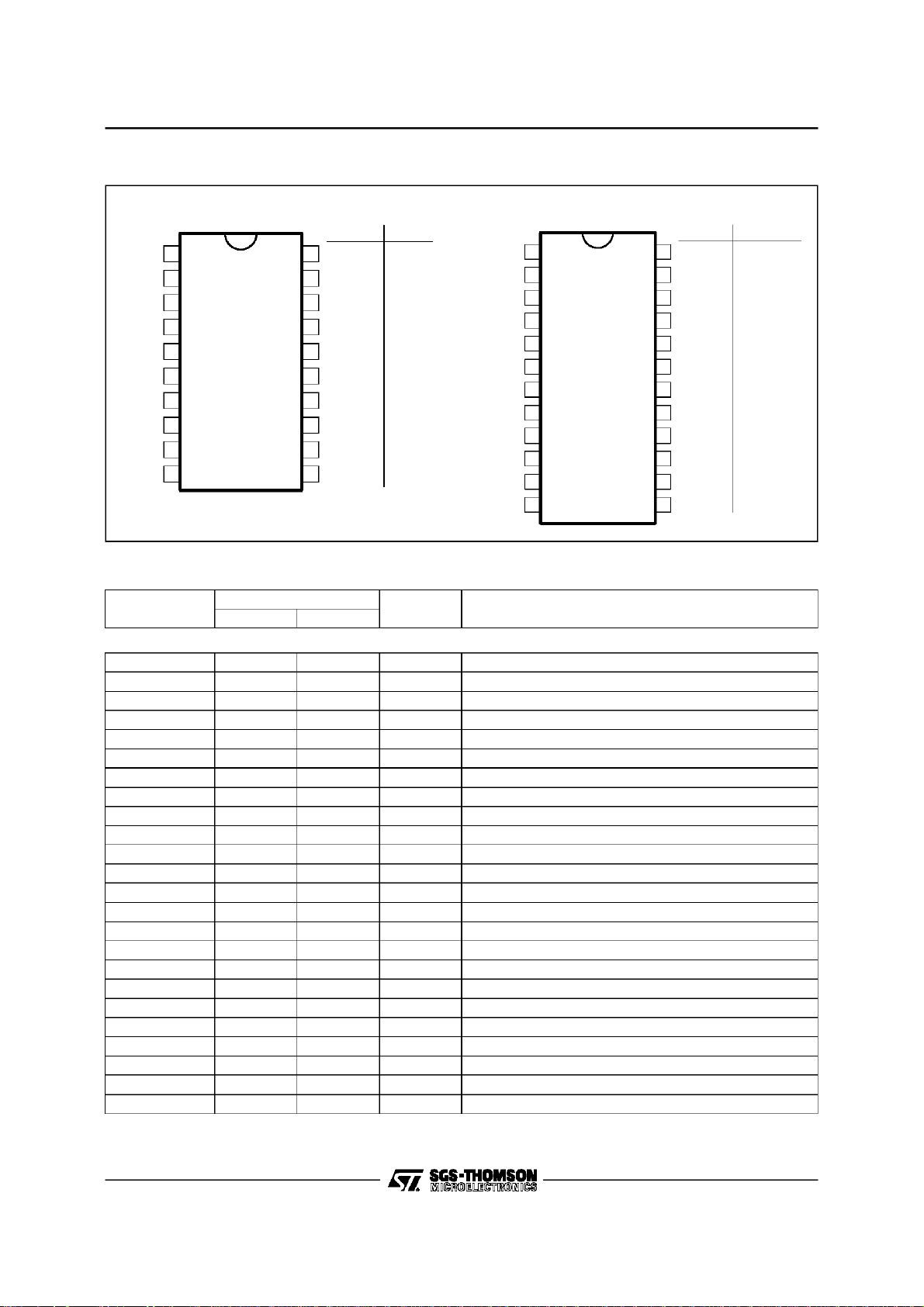
PIN CONNECTIONS
DIP20
CRT LCD
XTO
XTI
CKO
POR
NCS
SDA
SCK
V
REF
V
SSA
V
SS
1
2
3
4
5
6
7
8
9
10
20
19
18
17
16
15
14
13
12
11
V
DD
V
DD
SYNC IN CKD
V
C
-
I
B
G
R
Y
SYNC
SYNC
FRAME
LOAD
DF
D0
D1
D3
D2
V
EE
RESERVED
XTO
XTI
CKO
POR
NCS
SDA
SCK
V
REF
V
SSA
V
RESERVED
1
2
3
4
5
6
7
8
9
10
11
SS
12
PIN DESCRIPTION
o
Symbol
CRT MODE
- - 1 - Reserved
XTO 1 2 O Crystal oscillator output
XTI 2 3 I Crystal oscillator or clock input
CKO 3 4 O Clock output
POR 4 5 O Programmable output port
NCS 5 6 I Serial interface selection
SDA 6 7 I/O Serial data input/output
SCK 7 8 I Serial interface clock input
V
REF
V
SSA
V
SS
- - 12 - Reserved
- - 13 - Reserved
Y 11 14 O Luminance output
R 12 15 O Red output
G 13 16 O Green output
B 14 17 O Blue output
I 15 18 O Fastblanking output
- 16 19 O Reserved
C
SYNC
V
SYNC
SYNC IN 19 22 I/O Synchro input
V
DD
- - 24 - Reserved
Pin n
DIP20 SO24
I/O Description
8 9 I Resetinput and ref supply of Y DAC
9 10 S Ref ground of Y DAC
10 11 S Ground
17 20 O Composite synchro output
18 21 O Vertical synchro output
20 23 S +5v powersupply
SO24
CRT LCD
24
-
V
23
22
21
20
19
18
17
16
15
14
13
DD
SYNC IN
V
SYNC
SYNC
C
-
I
B
G
R
YV
-
RESERVED
V
DD
CKD
FRAME
LOAD
DF
D0
D1
D3
D2
EE
RESERVED
9410-01.EPS - 9410-02.EPS
9410-01.TBL
2/25
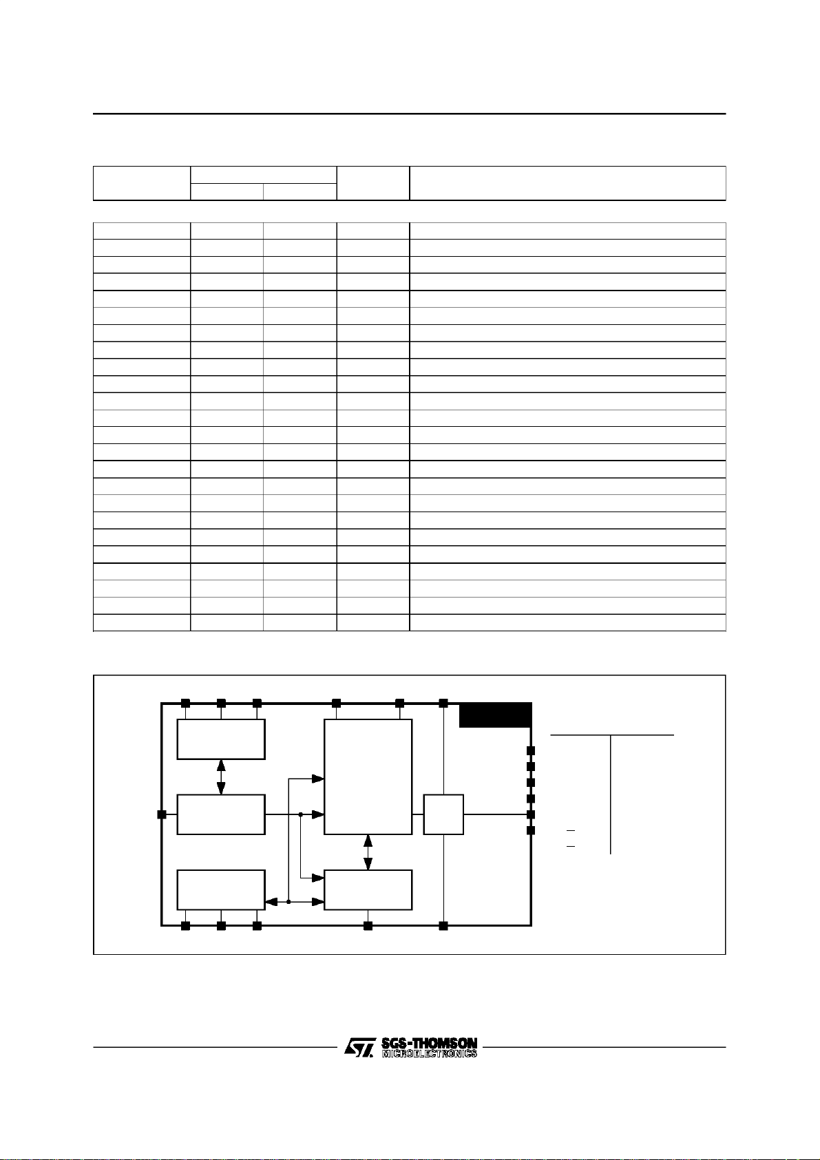
PIN DESCRIPTION(continued)
o
Symbol
LCD MODE
- - 1 - Reserved
XTO 1 2 O Crystal oscillator output
XTI 2 3 I Crystal oscillator or clock input
CKO 3 4 O Clock output
POR 4 5 O Programmable output port
NCS 5 6 I Serial interface selection
SDA 6 7 I/O Serial data input/output
SCK 7 8 I Serial interface clock input
V
REF
V
SSA
V
SS
- - 12 - Reserved
- - 13 - Reserved
V
EE
D2 12 15 O D2 Data output
D3 13 16 O D3 Data output
D1 14 17 O D1 Data output
D0 15 18 O D0 Data output
DF 16 19 O LCD polarity output
LOAD 17 20 O Load output (line)
FRAME 18 21 O Frame output
CKD 19 22 I/O Data Clock
V
DD
- - 24 - Reserved
Pin n
DIP20 SO24
I/O Description
8 9 I Resetinput and ref supply of contrast adjustment
9 10 S Ref ground of contrast adjustment
10 11 S Ground
11 14 O Constrast adjustment
20 23 S +5v powersupply
STV9410
9410-02.TBL
BLOCK DIAGRAM
GENERATOR
SYNC
IN
TIME BASE
INTERFACE
NCS SDA SCK
CLOCK
MCU
V
DD
CONTROL
PROCES SING
DISPLAY
LOGIC
6K BYTE
RAM
V
SS
PORCKOXTI XTO
V
REF
DAC
V
STV9410
SSA
CRT
MODE
C
SYNC
V
SYNC
I
Y
LCD
MODE
D2, D3, D1R, G, B
LOAD
FRAME
D0
V
EE
DF
CKD (SYNC IN)
9410-03.EPS
3/25

STV9410
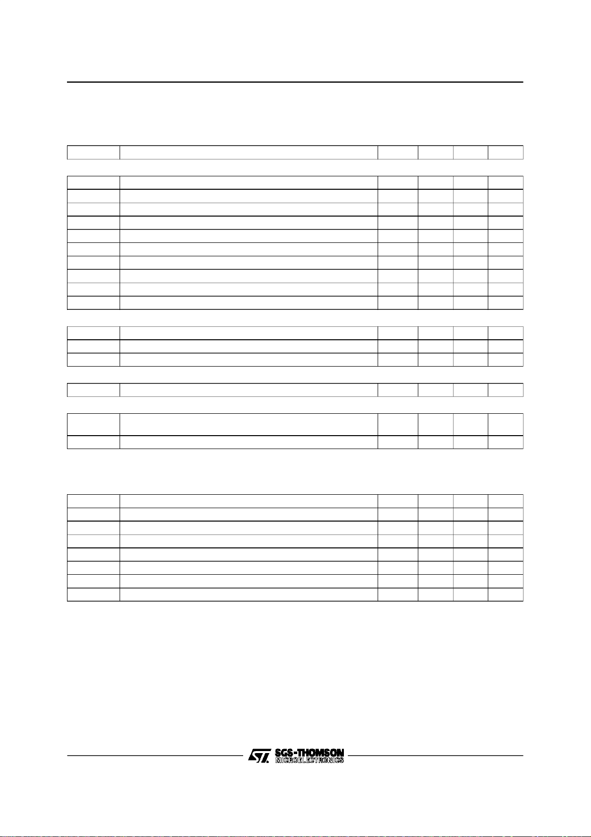
ABSOLUTEMAXIMUMRATINGS
Symbol Parameter Value Unit
* Supply Voltage -0.3, +7.0 V
V
DD
* Input Voltage -0.3, +7.0 V
V
IN
T
oper
T
stg
P
tot
* with respect to V
ELECTRICALCHARACTERISTICS
=5V,VSS=0V,Ta= 0 to +70oC, fxtal = 8 to 10MHz, unlessotherwise specified)
(V
DD
Symbol Parameter Min Typ Max Unit
V
DD
I
DD
INPUTS
NCS, SDA, SCK, SYNC IN, XTI
V
IL
V
IH
I
IL
C
IN
V
REF
V
rh
V
rst
R
IN
V
SSA
OUTPUTS
SDA, C
V
OL
V
OH
Y
L
I
L
D
Z
OUT
T
p
* no load on outputs
Operating Temperature 0, +70
Storage Temperature -40, +125
Power Dissipation 300 mW
SS
Supply voltage 4.75 5.0 5.25 V
Supply current * - - 50 mA
Input low voltage 0 - 0.8 V
Input high voltage (except XTI) 2 - V
Input leakage current (except XTI) (0 < VIN<VDD) -10 - +10 µA
Input capacitance (except XTI) - 10 - pF
Voltage reference of DAC 1.5 - V
Reset level on V
V
to V
REF
internal resistance 0.4 - 1.0 kΩ
SSA
REF
0 - 0.4 V
Reference level of DAC 0 - V
SYNC,VSYNC
, R, G, B, I, SYNC IN, DF, XTO, CKO, POR
Output low voltage (IOL= 1.6mA) 0 - 0.4 V
Output high voltage (IOH= - 0.1mA ) 0.8 V
Output voltage (V
REF
=5V, V
SSA
=0, I
OUT
=0)
-VDDV
DD
Integral linearity - - 0.25 V
Differential linearity - - 0.1 V
Output impedance - - 0.5 kΩ
Propagation time at V
OUT
=20pF, I
C
L
90% of V
OUT
FINAL
=0, V
,
REF
=5V, V
SSA
=0V
- - 80 ns
DD
DD
DD
o
C
o
C
9410-03.TBL
V
V
V
9410-04.TBL
4/25
STV9410
TIMINGS
=5V±5%, VSS=0V,Ta= 0 to + 70oC, fxtal = 8 to 10MHz,
(V
DD
= 0.8V,VIH=2V,VOL= 0.4V,VOH= 2.4V,CL=50pF,unless otherwisespecified)
V
IL
Symbol Parameter Min Typ Max Unit
SERIAL INTERFACE NCS, SCK, SDA (Figure 1)
T
csl
T
sch
T
scl
f
SCK
T
sds
T
sdh
T
sdv
T
sdx
T
sdz
T
read
OSCILLATOR INPUT (XTI) (Figure 1)
T
wh
T
wl
F
clk
RESET (V
T
res
OUTPUT SIGNALS SDA, C
T
ph,Tpl
T
skew
NCS low to SCK fallingedge 0 ns
SCK pulsewidth high 80 ns
SCK pulsewidth low 80 ns
Serial Clock Frequency 4 MHz
Set up time of SDA on SCK rising edge 20 ns
Hold time of SDA after SCK rising edge 20 ns
Access time in read mode 50 ns
Hold data in read mode 0 ns
Serial interface disable time 50 ns
Delay before Valid Data 2 µs
Clock high level 30 ns
Clock low level 30 ns
Clock frequency 8 10 MHz
)
REF
Reset Low level pulse 2 µs
SYNC,VSYNC
, R, G, B, I, SYNC IN, DF, XTO, CKO, POR (Figure 2)
Propagation time CL=30pF
= 100 pF
C
L
100
Skew between R, G, B,I signals 30 ns
50
ns
ns
(VDD=5V±5%, VSS=0V,Ta= 0 to + 70oC, fxtal = 8 to10MHz,
= 0.2VDD,VOH=0.8VDD,CL=100pF,unless otherwisespecified)
V
OL
LCD INTERFACE D0, D1, D2, D3, CKD, LOAD, DF, FRAME (Figure 3)
t
CYC
t
t
t
WLD
t
t
t
t
SUF
CH
CL
SU
DH
DF
CKD Shift Clock Period 4 x Pxtal ns
CKD Clock High 150 ns
CKD Clock Low 150 ns
Load Pulse Width 150 ns
Data Set-up Time 150 ns
Data HoldTime 150 ns
DF Delay from Load 100 ns
Frame Set-up before Load 150 ns
9410-05.TBL
5/25
STV9410
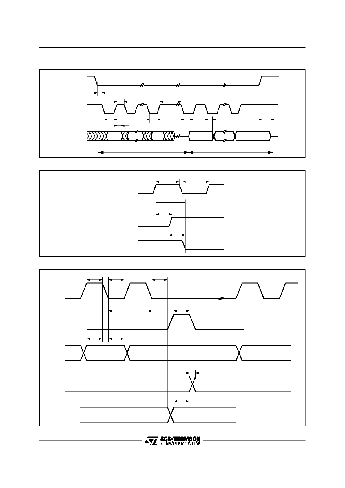
Figure1 : MicrocontrollerInterfaceTimings
NCS
t
csl
t
sch
SCK
t
sds
SDA
A8 A9 A6 A7 D0 D1 D6 D7
Figure2 : Output Signals Delay versus Clock
t
scl
t
sdh
WRITE READ
t
read
t
sdv
t
sdx
t
sdz
9410-04.EPS
Figure3 : LCD Interface Timings
CKD
LOAD
t
CH
t
SU
t
CL
t
DH
XTI
OUTPUT
OUTPUT
t
CYC
t
t
CLD
ph
t
wh
t
pl
t
skew
t
WLD
t
wl
9410-05.EPS
6/25
D0, D1
D2, D3
DF
FRAME
t
SUF
t
DF
9410-06.EPS

STV9410
2. FUNCTIONALDESCRIPTION
STV9410displayprocessoroperationis controlled
by a host microcomputervia a 3-wire serial bus. It
is fully programmable through seven internal
read/write registers and performs all the display
functions either for CRT screen or LCD passive
matrix by generatingpixels from data stored in its
internal memory. In addition, the host microcomputer can have straightforward accesses to the
on-chip 6 Kbytes RAM, even during the display
operation.
The following functions are integrated in the
STV9410:
- Crystal oscillator,
- Programmable timing generator,
- Microcomputer3-wire serial interface,
- ROM charactergeneratorincluding128alphanumeric and 128 semigraphic character sets,
- 6 Kbyteson chipRAM to storecharactercodes,
user definable character sets, and any host microcomputerdata,
and in CRT mode :
- Y outputdriven by a 4-bitDAC,
- Programmablemaster or slave synchromodes,
- R, G, B,I outputs,
in LCD mode:
- LCD interface for passive multiplexedmatrix,
- 7 grey levels plus black.
2.1 SERIALINTERFACE
This 3-wire serial interface can be used with any
microcomputer.Datatransferissupportedbyhardware peripherals like SPI or UART and can be
emulated with standard I/O port using software
routine ( seeapplicationnote ).
NCSinputenablestransferonhighto lowtransition
and transfer stays enabled as long as NCS input
remains at logical low level. NCS input disables
transfer as soon as low to high transition occurs,
whatever transfer state is, and transfer remains
disabled as long as NCS input remains at logical
high level.
SCKinput receives serial clock; it must be high at
the beginning of the transfer; data is sampled on
rising edge of SCK.
SDAinput(in writemode)receivesdatawhichmust
be stable at least t
before and at least t
sds
sdh
after
SCK rising edge. In read mode, SDA receives
address and read command (R/W bit) and then it
switches from input state to output state to send
data (seeData transferand ApplicationNote).
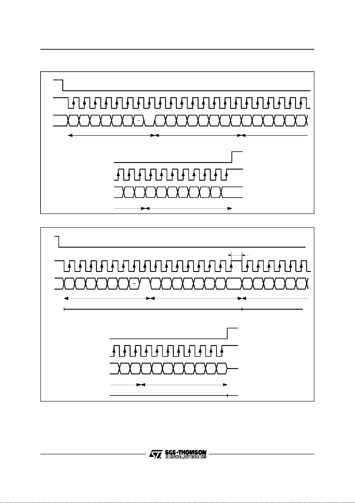
Data Transfer in Write Mode
The host MCU writesdata into STV9410registers
or memory.TheMCU sendsfirstMSBaddresswith
R/W bit clear, it sends secondly LSB address followed by data byte(s). STV9410, then, internally
incrementsreceived address,readyto storeasecond databyteif needed,and soon, aslongasNCS
remainslow (see Figure 4). LSBare sent first.
Data Transfer in Read Mode
The host MCUreads data from STV9410 registers
or memory.TheMCU sendsfirstMSBaddresswith
R/W bit set, it sends secondly LSB address, then
SDA pin switches from input state to output state
and providesdatabyte(s) at SCK MCU clock rate.
Notice that a minimum delay is needed before
sendingthefirst SCKrisingedgeto sample the first
data bit (at least 2µs). After each data byte
STV9410 internally increments address and it
sendsnextdataatSCKfrequency.SDAremainsin
output state as long as NCS remains low (see
Figure5).
Address auto-incrementation allows host MCU to
use 8, 16, 32-bit data words to optimize transfer
rate. LSBare sent first. SCK max speed is 4MHz.
7/25
STV9410
Figure4 : Serial InterfaceWrite Mode
NCS
SCK
SDA
A8 A9 A10 A11 A12 A13 W A0 A1 A2 A3 A4 A5 A6 A7 D0 D1 D2 D3 D4 D5
@ MSB @ LSB Data byte 1
NCS
SCK
D5 D6 D7 D0 D1 D2 D3 D4 D5 D6 D7
SDA
Figure5 : SerialInterface Read Mode
NCS
SCK
SDA
A8 A9 A10 A11 A12 A13 R A0 A1 A2 A3 A4 A5 A6 A7 D0 D1 D2 D3 D4 D5
data byte ndata byte n - 1
9410-07.EPS
2µs min.
SDA Pin
8/25
@ MSB @ LSB Data byte 1
INPUT OUTPUT
NCS
SCK
D5 D6 D7 D0 D1 D2 D3 D4 D5 D6 D7
SDA
data byte ndata byte n - 1
SDA Pin
OUTPUT
INPUT
9410-08.EPS
 Loading...