

SGS Thomson Microelectronics STV9306 Datasheet
BUS CONTROLLEDVERTICALDEFLECTION SYSTEM
WITH EAST/WESTCORRECTIONOUTPUT CIRCUIT
.
FULLYI2C CONTROLLED
.
DMOSPOWER HALF-BRIDGEAMPLIFIER
.
DC COUPLEDOPERATION
.
INTERNALFLYBACKGENERATOR(UPTO60V)
.
SELFADAPTEDSAWTOOTH(50/60Hz)
.
100HzOPERATION
.
VERTICAL LINEARITY, AMPLITUDE AND
CENTERING ADJUSTMENTS
.
HORIZONTAL WIDTH, PINCUSHION,
TRAPEZOIDAND CORNERADJUSTMENTS
.
BREATHING CORRECTION
.
4/3, 16/9 CRTAPPLICATION
.
THERMALPROTECTION
.
LINEARVERTICALZOOMFUNCTION
.
E/W CLASSAOUTPUT
.
LOW EXTERNALCOMPONENTS
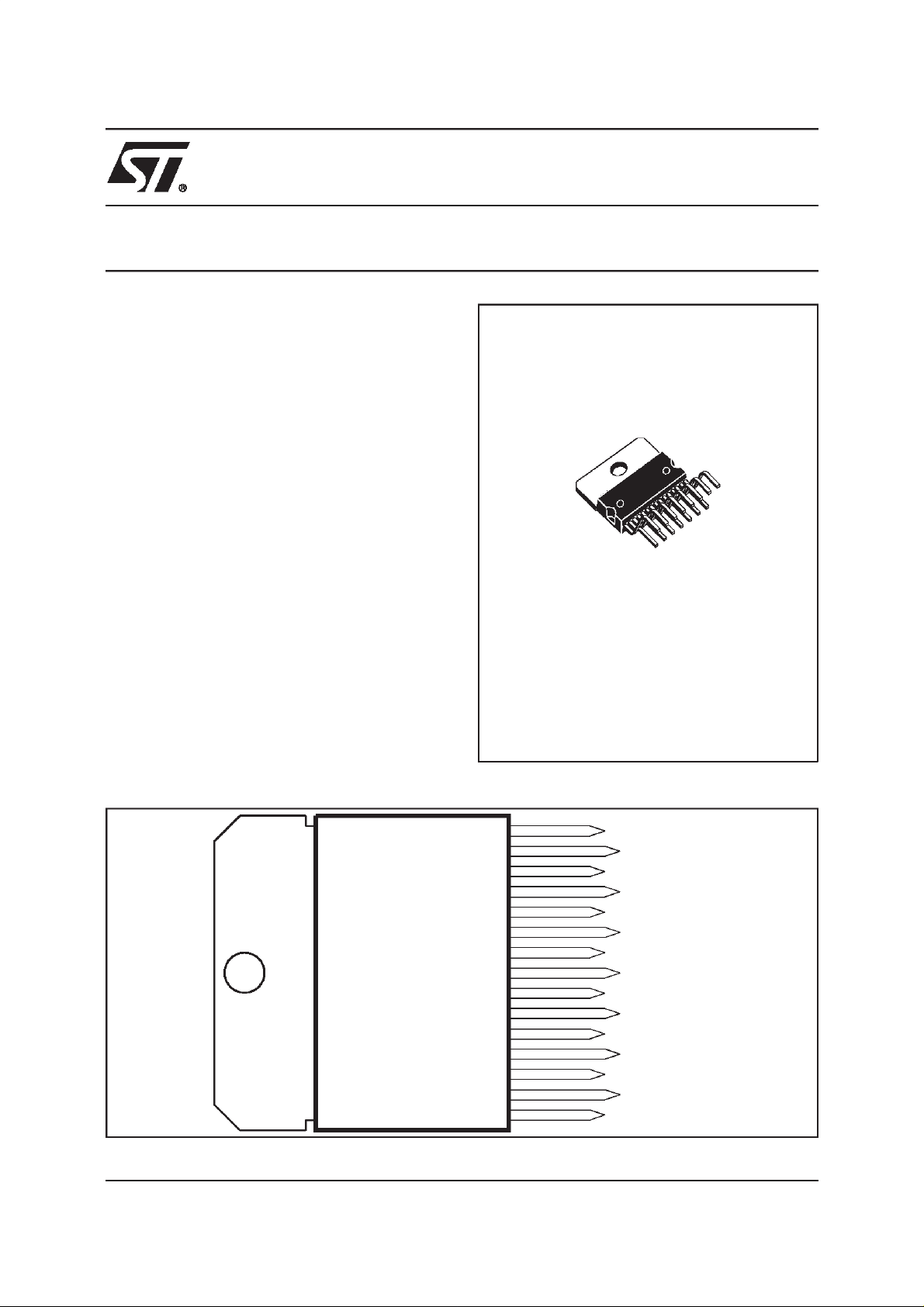
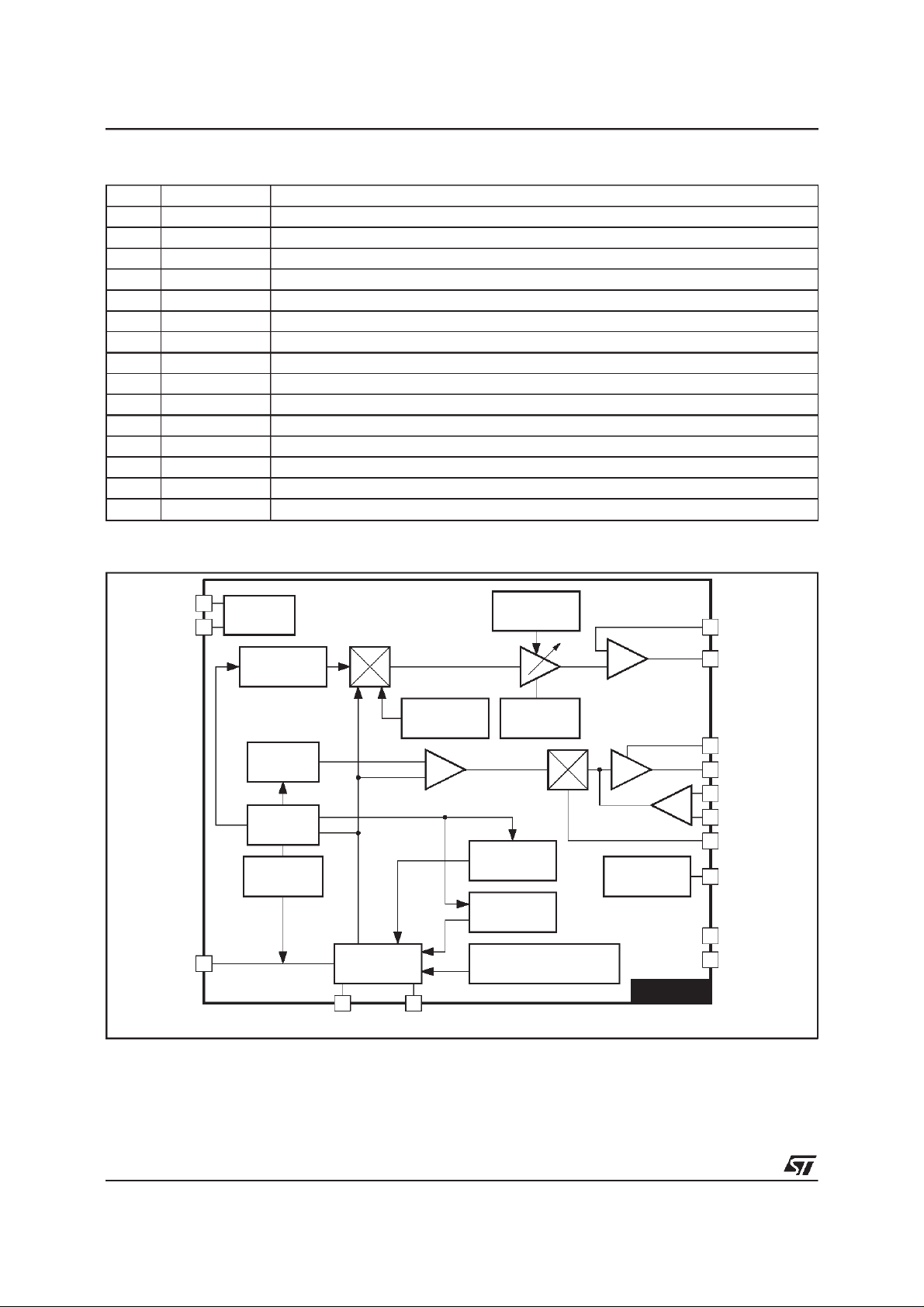
MULTIWATT15
(PlasticPackage)
ORDER CODE :
STV9306
PRELIMINARY DATA
STV9306
DESCRIPTION
2
The STV9306 is a fully I
deflection IC designed for use in 110°,4/3 or 16/9
CRT applications. It integrates both the vertical
deflection and E/W correction circuitries necessary in design of a 110°chassis.
PIN CONNECTIONS
C controlled vertical
15
14
13
12
11
10
BREATHING
SENS1
EWFB
SENS2
EWOUT
VOPS
9
8
7
6
5
4
3
2
1
OUT
GND
FLYBACK
V
S
SYNC
CHOLD
SDA
CRAMP
SCL
9306-01.EPS
December 1998
This isadvance informationon a newproductnow in developmentor undergoingevaluation. Detailsare subject to change without notice.
1/12
STV9306
PIN LIST
Pin Symbol Description
1 SCL I
2 CRAMP Ramp Capacitor
3 SDA I
4 CHOLD Hold Capacitor
5 SYNC Sync Input
6 VS Supply Voltage
7 FLYBACK Flyback Output
8 GND Ground
9 OUT Vertical Output
10 VOPS Vertical Output Power Supply
11 EWOUT EW Output
12 SENS2 Vertical Current Sense 2
13 EWFB EW Feedback
14 SENS1 Vertical Current Sense 1
15 BREATHING Breathing Input
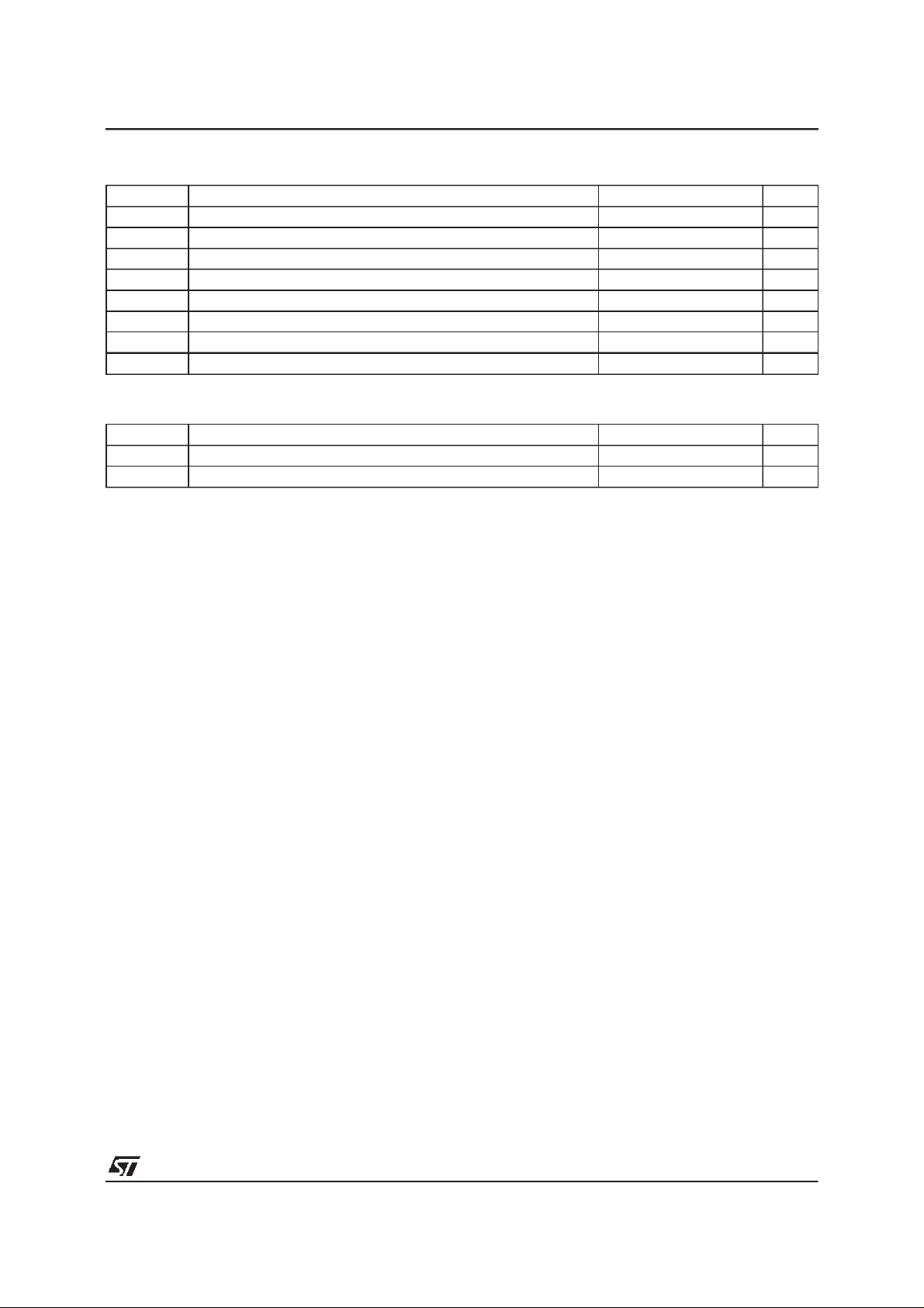
BLOCKDIAGRAM
2
C Bus Clock
2
C Bus Data
9306-01.TBL
SDA
SCL
SYNC +
OVERSIZE
3
1
5
BUS
DECODER
TRAPEZIUM
CORRECTION
VERTICAL
SHIFT
V MIDDLE
SCREEN
OVERSIZE
BLANKING
CORNER
CORRECTIONEWAMPLITUDE
RAMP
GENERATOR
2
CRAMP CHOLD
4
HORIZONTAL
WIDTH
C
CORRECTION
S
CORRECTION
VERTICALAMPLITUDE
ADJUSTMENT& FORMAT
FLYBACK
GENERATOR
STV9306
13
EWFB
11
EWOUT
10
VOPS
9
OUT
14
SENS 1
12
SENS 2
15
BREATHING
7
FLYBACK
8
GND
6
V
S
9306-02.EPS
2/12
STV9306
ABSOLUTE MAXIMUMRATINGS
Symbol Parameter Value Unit
V
S
V
OUT
V
V
IS
E/W OUT East/West Output 60 V
T
oper
T
stg
T
THERMALDATA
Symbol Parameter Value Unit
R
th (j-c)
T
Supply Voltage 35 V
Flyback Peak Voltage 60 V
Input Voltage at Pins 1-3-5-12-13-14-15 -0.3, V
I
Input Voltage at Pins 2-4 10 V
Operating Temperature -10, +70
Storage Temperature -55, +150
Junction Temperature +150
j
Junction-case Thermal Resistance Max. 3
Temperature for Thermal Shutdown Min. 140
t
S
o
o
o
o
C/W
o
V
C
C
C
9306-02.TBL
C
9306-03.TBL
3/12
STV9306
ELECTRICALCHARACTERISTICS
= 24V,R
V
S
Symbol Parameter Test Conditions Min. Typ. Max. Unit
SUPPLY
V
S
I
S
RAMP GENERATOR CONTROL
V
Rlow
t
D
I
ISY
V
THSY
I
OB
POWER AMPLIFIER
I
IBR
V
BREATH
V
7H
V
7L
I
SENS1
I
SENS2
V
9H
V
9L
/st
dV
9H
/dt
dV
9L
VERTICAL OUTPUT (Pin 9)
I
PP
I
DC
Z
SLP
I
SC
I
CC
BR
EAST/WEST CORRECTION (V_SAW = 100000, V_SH = 10000, V_SC = 0000, V_CC = 1000) (see Figure 6)
I
BIAS
V
PAR
V
DCEW
Trap Trapezium Correction at Pin 13 (see Figure 9)
Shape Parabola Shape (cornercorrection) at Pin 13
V
11L
= 0.5Ω, Normal mode, T
SENS
=25oC, unless otherwise specified
amb
Operating Supply Voltage 16 28 V
Supply Current on Pins 6-10 IO= 0 40 60 mA
Minimum V
Voltage atPin 2 1.8 2 2.2 V
RAMP
Discharge Time at Pin 2 50 µs
Synchro Input Current at Pin 5 VSY= 0 -6 -3 µA
Synchro Threshold Voltage at Pin 5 2.5 3 3.5 V
Oversize Blank Input Current at Pin 5 70 100 µA
Breathing Current Input Current at Pin 15 V
= 0V -10 -5 µA
BREATH
Breathing Operating Voltage atPin 15 0 9 V
Saturation Voltage to supply at Pin 7 IO= -1.5A, V9>VS+ 5V 2.5 3.5 V
Saturation Voltage to Ground atPin 7 IO= 100mA 1.5 2.5 V
-20
Bias Input Current at Pin 14
Bias Input Current at Pin 12
V14=0V
=0V
V
12
-20
-10
-10
Saturation Voltageto supply at Pin 9 versus Pin 10 IO= -1.5A 2.5 3.5 V
Saturation Voltage to Ground atPin 9 IO= 1.5A 1.5 2.5 V
Vertical Deflection Current (see Figure 1) V_SAW = 000000
V_SAW = 111111
Average Current (vertical shift)
at V_SAW = 111111
slope in zoom mode
Z
=
SLP
slope in normal mode
(see Figure 2)
V_SH = 01111
V_SH = 11111
V_ZOOM =000
V_ZOOM =111
S Correction = ISC/IPP(see Figure 3) V_SC = 0000
V_SC = 1111
C Correction = ICC/IPP(see Figure 4) V_CC = 0111
V_CC = 1111
I
− I
PP
Breathing BR =
PPB
I
PP
(see Figure 5)
BR
BR
Min.V15
Max.V15
=9V
=1V
+10
+5
1.8
3
-0.35
0.35
106
130
0
6
-3
3
0
10
mV/°C
mV/°C
Input Bias Current at Pin 13 -1 -0.5 µA
Parabola Amplitude (pincushion correction)
at Pin 13(see Figure 7)
Horizontal Width Adjustment at Pin 13
(see Figure 8)
Trap = V
(see Figure 10) - Shape = V
PARTUP/VPARTLOW
COR/VPAR
Saturation Voltage I
EW_AMP = 00000
EW_AMP = 11111
EW_DC = 00000
EW_DC = 11111
HShrink active
EW_TRAP = 01111
EW_TRAP = 11111
EW_SHAPE = 00000
EW_SHAPE = 11111
= 500mA 2 V
OUT
0
5
1
6
+6
0.6
1.7
0
50
µA
µA
A
A
A
A
%
%
%
%
%
%
%
%
V
V
V
V
V
%
%
9306-04.TBL
4/12
 Loading...