

SGS Thomson Microelectronics STV8224B Datasheet
MULTISTANDARDVIDEO AND SOUND IF SYSTEM
WITHAUDIO AND VIDEO SWITCHES
.
VIDEOPLLDEMODULATION
.
SOUNDPLLDEMODULATION
.
POSITIVEANDNEGATIVEMODULATION
.
AGC FOR BG AND L STANDARDS
.
AUDIO SWITCH
.
DC VOLUME CONTROL
.
VIDEOSWITCH
DESCRIPTION
TheSTV8224Bis a pictureandsoundIFprocessor
formultistandardapplicationwith very fewexternal
componentsand adjustments.
It provides the audio and video switches for one
SCART plug application.
AM sound demodulation is performed with the
STV8225add-on.
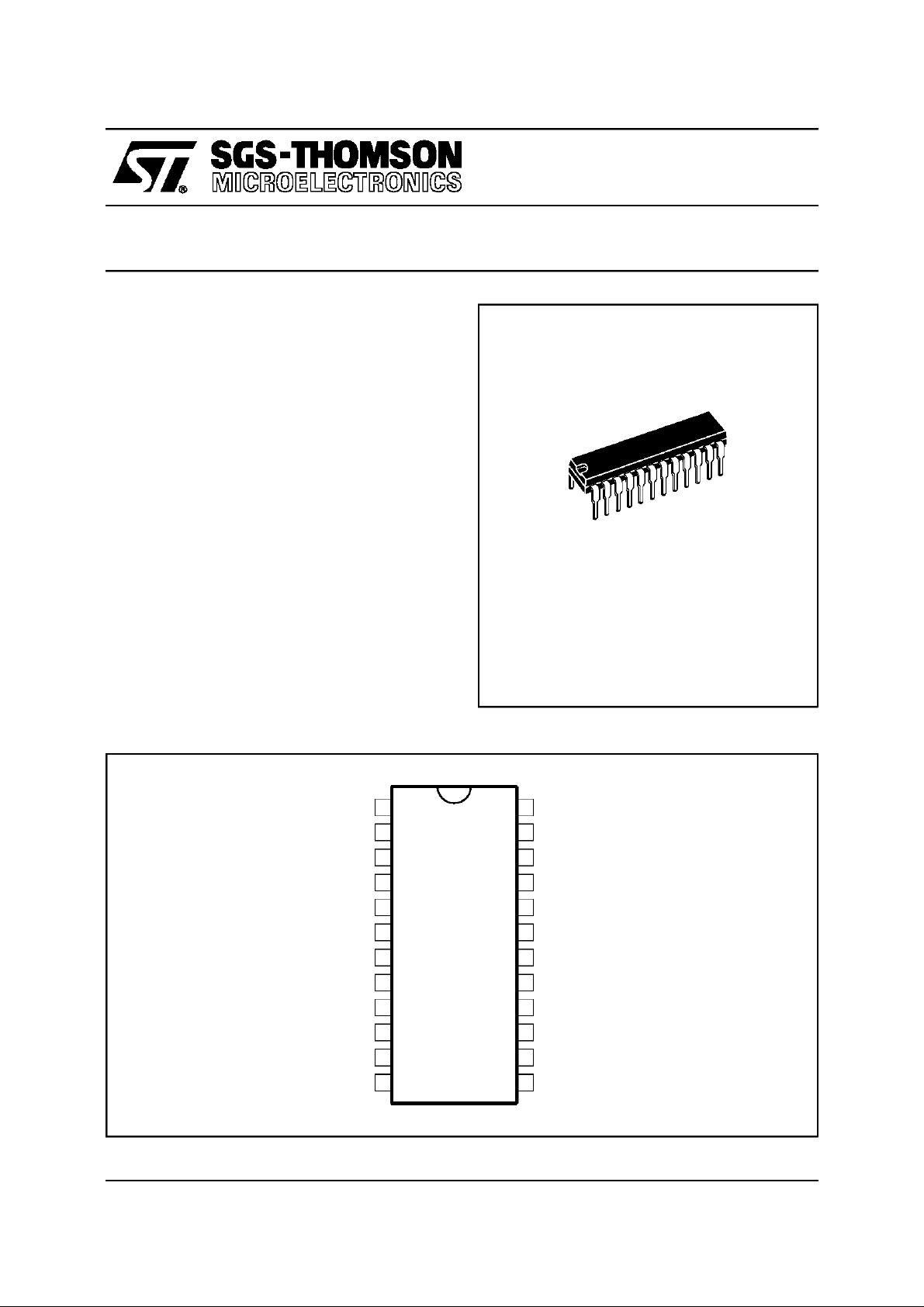
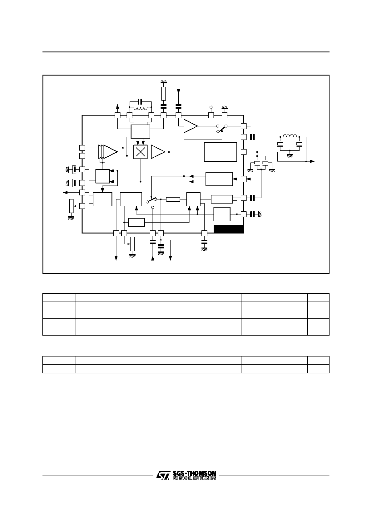
SHRINK24
(PlasticPackage)
ORDER CODE :
STV8224B
STV8224B
PIN CONNECTIONS
PIF PLL FILTER
AFC OUTPUT
CVBS OUTPUT
SWITCHINGINPUT (STANDARD + INT/EXT)
IF LC
IF LC
AUDIO HIGH PASS FILTER
2nd IF SOUND INPUT
AUDIO AND 2nd IF DECOUPLING
INTERNALVIDEO INPUT
VIDEO SWITCH OUTPUT
EXTERNAL VIDEO INPUT
January 1997
1
2
3
4
5
6
7
8
9
10
11
12
24
TUNER AGC STARTING POINT ADJUSTMENT
23
TUNER AGC OUTPUT
22
AGC CAPACITOR
21
AGC CAPACITOR (L STANDARD)
20
IF INPUT
19
IF INPUT
18
GROUND
17
V
CC
16
EXTERNAL AUDIO INPUT
15
FM DEMODULATEDAUDIO OUTPUT
14
AUDIO SWITCH OUTPUT
13
VOLUME CONTROL + MUTE
8224B -01.EPS
1/12
STV8224B
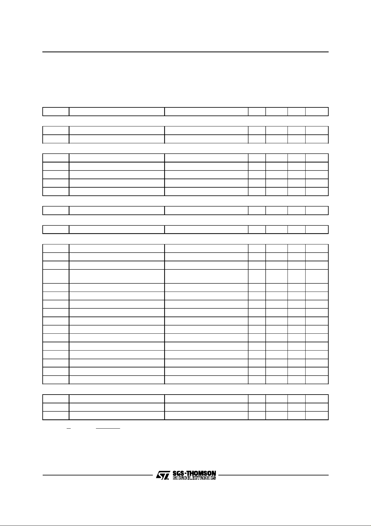
BLOCKDIAGRAM
AFC
OUTPUT
PIF PLL
& AFC
EXT
CVBS
6dB
V
CC
1817125162
SWITCHED
11
CVBS
10
IF INPUT
TUNER
AGC
OUTPUT
19
20
21
AGC
22
23
TUNER
AGC
24
SWITCHED
DC
VOLUME
MUTE
14 13 15 7
AUDIO
VID
AMP
16
EXT
AUDIO
AUDIO
OUT
Int/Ext
BG/L
SIF
PLL
WHITE NOISE
&
SPOT INVERT
LOGIC
INTERFACE
LIMITER
AUDIO
Vref
STV8224B
3
SFE
5.5
4
8
9
SFE
6.5
ABSOLUTE MAXIMUMRATINGS
Symbol Parameter Value Unit
V
S
Vx Tuner AGC Voltage V
T
stg
T
oper
Supply Voltage 13.5 V
CC
Storage Temperature -40, +150
Operating Temperature 0, +70
CVBS
OUT
V
o
C
o
C
8224B -02.EPS
8224B-01.TBL
THERMAL DATA
Symbol Parameter Value Unit
Junction-ambient Thermal Resistance Max. 75
2/12
R
th (j-a)
o
C/W
8224B-02.TBL
STV8224B
ELECTRICAL CHARACTERISTICS
(T
=25°C, VCC= 9V,IFinput= 10mV
amb
VideomodulationDSB,D = 90%at B/G,D = 95%at L,f
VideoBW= 5MHz,Soundcarrier input: 5.5MHz,10mV
Volumeattenuation= 0dB,unlessotherwisespecified)
Symbol Parameter Test Conditions Min. Typ. Max. Unit
SUPPLY
V
I
CC
IF AMPLIFIER
V
19-20
R
19-20
C
19-20
Gr Gain Control Range 68 dB
SYNCHRONOUS VIDEO DEMODULATOR
DF
AFC
S2 AFC Slope See Figure 21 0.2 µA/kHz
DEMODULATED VIDEO OUTPUT (Pin 3)
V
BG vs L Amplitude Difference 10 %
V
BW Bandwidth -3dB Video Signal 7 9 MHz
Dg Differential Gain 6 8 %
Dp Differential Phase 3 6 Degree
Vr3c Residual Carrier Signal (RMS Value) 1 10 mV
Vr3h Residual 2nd Harmonic (RMS Value) 1 10 mV
S/N Signal to Noise Ratio Note 1 - Weighted CCIR-567 56 61 dB
V
WTH
V
V
BTH
V
AGC CIRCUIT (BG MODE)
I
22CBG
I
22DBG
C/D Charging/Discharging Ratio 45
Notes :
Supply Voltage 8 9 12.6 V
CC
Supply Current I17,VCC=9V 70 95 mA
Input Sensitivity (RMS) -3dB Video at Output 70 µV
Differential Input Resistance 2 kΩ
Differential Input Capacitance 2 pF
Max Input Signal +1dB Video at Output 180 mV
Vision Carrier Capture -1.4 1.6 MHz
PC
Amplitude TopSync to White 2 2.3 2.6 V
A3
Top Sync Level B/G and L 1.6 1.9 2.2 V
S3
Zero Carrier Level B/G
Internal Bias of Emitter Follower 3 5 mA
I
3
Intermodulation 1.07MHz Note 2 52 dB
White Noise Threshold Voltage 4.85 V
White Noise Insertion Level 3.6 V
WIL
Black Noise Threshold Voltage 1.3 V
Black Noise Insertion Level 2.5 V
BIL
Charging Current 550 950 1300 µA
Discharge Current 12 20 28 µA
S
=
1.
20 log 10
N
2. Video carrier relative level = 0dB, Chroma subcarrier level = -3.2dB, Sound carrier relative level = -20dB.AGC voltage (Pin 22)
is adjustedto get 1V
V
out black white
(
V
mV
N
atBW = 5MHz
)
RMS
signalon output (Pin 3).
PP
synclevelat B/G, Peak-whitelevelat L,
RMS
=38.9MHz,fSC= 33.4MHz,
PC
RMS,fM
=1kHz,AudioBW= 20kHz,∆f=±50kHz,
L
4.4
1.8
RMS
RMS
PP
V
V
8224B-03.TBL
3/12
STV8224B
ELECTRICAL CHARACTERISTICS
=25°C,VCC= 9V, IF input= 10mV
(T
amb
VideomodulationDSB,D = 90% atB/G,D = 95% at L, f
VideoBW=5MHz,Soundcarrierinput: 5.5MHz,10mV
(continued)
synclevelat B/G,Peak-whitelevelat L,
RMS
= 38.9MHz,fSC=33.4MHz,
PC
RMS,fM
=1kHz,AudioBW= 20kHz,∆f=±50kHz,
Volumeattenuation= 0dB, unlessotherwisespecified)
Symbol Parameter Test Conditions Min. Typ. Max. Unit
AGC CIRCUIT (L MODE)
I
22CL
I
22DL
I
22CL
I
22DL
TUNER AGC
I
23
S23 Current Slope R
I
23+
FM SOUND DEMODULATION
V
8S
R
AMR Amplitude Modulation Rejection Note 5 50 61 dB
SVR Supply Voltage Rejection Ratio Ripple signal : 100Hz, 0.5V
V
15
THD Total Harmonic Distortion 0.2 1 %
R
15
S/N Signal to Noise Ratio See Note 6,
Charging Current Note 3 2 3.3 4.5 mA
Discharge Current 0.3 µA
+ Additional Charging Current L in case of missing, VITS Pulses
5 µA
and no White in Video Content
Threshold Voltage Level for
Refered to Pin 3 2.75 V
Additional Charging Current
+ Additional Discharging Current 28 40 56 µA
Threshold Voltage Level for
Refered to Pin 3 2.25 V
Additional Discharging Current
Maximum Sinked Current 1.5 2 2.5 mA
=5kΩ 100 170 230 µA/dB
24
Maximum Tuner Plus Sinked
Note 4 40 mA
Current
Input Sensitivity 150 µV
Limiter Input Resistance 600 Ω
8
DC Voltage (Pin 8) 4.2 V
PP
28 33 dB
Detected AudioOutput Signal 0.85 1.1 1.4 V
Internal Deemphasis Resistor 600 750 900 Ω
55 60 dB
Weighted CCIR 468-4,
(quasi peak level) input Pin 8
Black Picture (sync only) Measurement between IF input
White Picture 46 50 dB
250kHz Square Wave 47 52 dB
(Pins19-20) and audiooutput(Pin 15)
SAW : K2955
BPF : SFE5.5MB
47 52 dB
RMS
RMS
VOLUME CONTROL
Range Control Range SeeFigure 22 72 77 dB
V
C
Notes : 3. Triggeredon white level
4. Additional sinked current forlarge increasing steps of input signal when:
- VoltagePin 22 > starting point defined Pin 24.
- Outputsignal (Pin 3) saturated(V
5. AMR = 20 log
S
6.
= 20 log
N
(mV
V
RMS
RMS
)
RMS
AM
)
(dB)
)
V
15
(mV
V
15
V
(mV
N
< V BTH inBG mode, V3> V WTH in L mode).
3
(dB) where VAM= output amplitude in AM for fM= 1kHz and m = 30%
4/12
8224B-04.TBL
 Loading...