


STV7801S
PLASMA DATA POWER SWITCH
PRELIMINARY DATA
FEATURES
■ High Voltage - Low Power Pulse Generator
■ 100V Absolute Maximu m Supply
■ High Load Drive Capability (25nF)
■ 5V Compatible Input Logic
■ Very Low Stand-by Current
■ Power Recovery High Current (±7A)
■ Totem Pole High Output Current (±5A)
■ Built-in Timing Control & Thermal Protection
■ BCD Technology
■ Packaging: Multiwatt 15, Power SO20
DESCRIPTION
STV7801 is a m onolithic integrated circuit implemented in STMicroelectronics BCD proprietary
technology designed as a switched power supply
generator for data drivers in a Plasma Display
Panel (P.D.P.) application.
The high load drive capabil ity of the STV7 801 reduces the number of devices necessary to drive a
complete PDP (4 to 6 devices for a 42” VGA 16/9
PDP monitor).
The STV7801 high current drive capability provides a high power recovery efficiency coefficient
superior to 85% on constant capacitive load.
To limit the numbe r of external components, the
device integrates level shifters driven with 5V
CMOS compatible levels.
To increase the reliability of the system, the device
integrates several protections such as output
over-voltage, over-temperature, power-ON protection.
.
MULTIWATT 15 (Plastic Package)
ORDER CODE: STV7801S
Customer samples will be available
by september 2000
POWERSO20 (Plast ic Package)
20 leads
ORDER CODE: STV7801SP
Revision 3.3
June 2000 1/18
This is preliminary information on a new product in development or undergoing evaluation. Details are subject to change without notice.
1

STV7801S
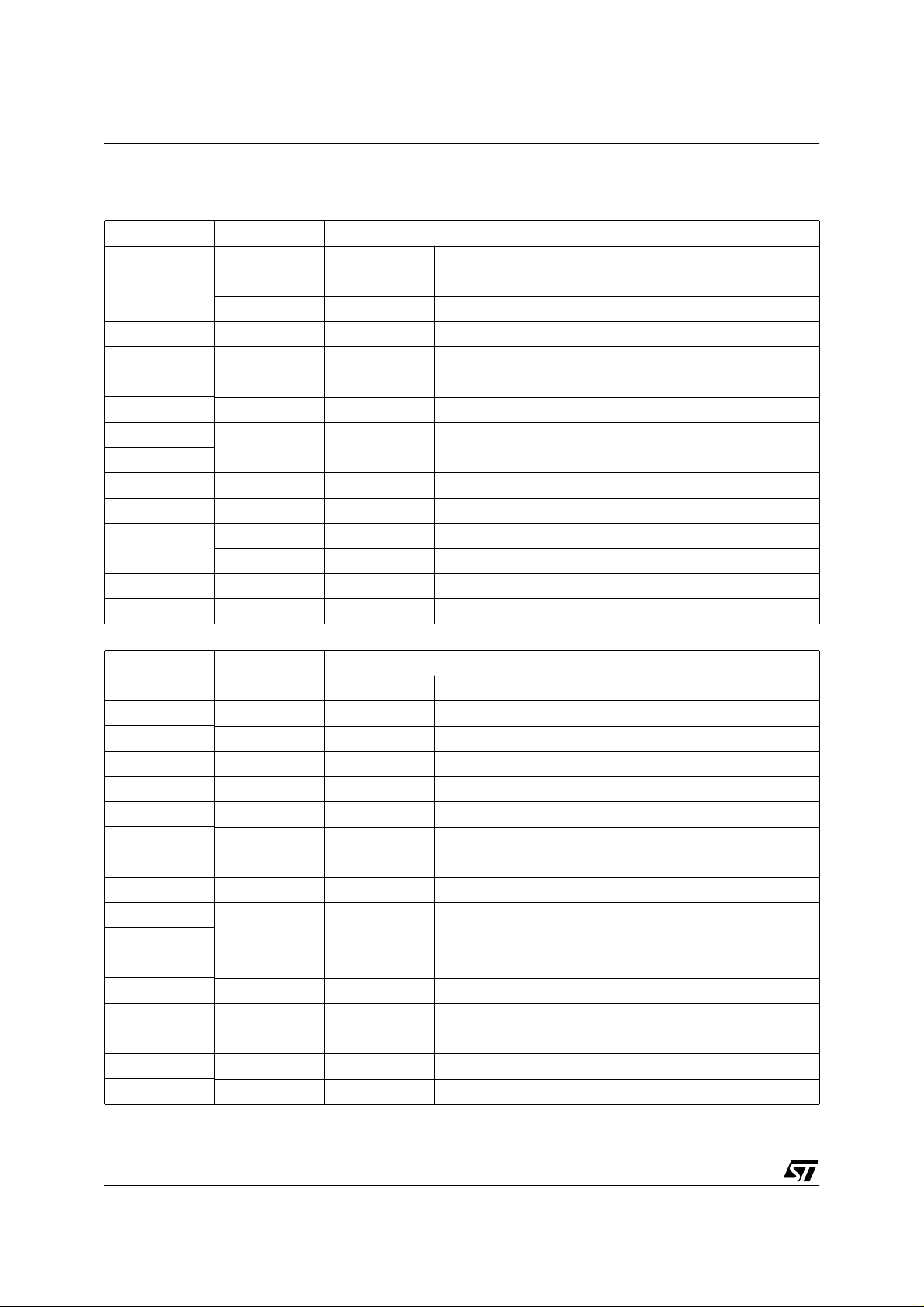
1 - PIN CONNE CT ION
Multiwatt 15
PowerSO20
15
14
13
12
11
10
Vpp
Vpp
CBoot
Out
Vssp
Vdd
9
8
7
6
5
4
3
2
1
DM-LH
Vsslog
PR
DM-HL
PR-FPS
LH-Tr
L-Clmp
H-Clmp
HL-Tr
2/18
Vsssub
HL-Tr
H-Clmp
L-Clmp
LH-Tr
PR-FPS
PR-FPS
DM-HL
PR
Vsssub
1
2
3
4
5
6
7
8
9
10
20
19
18
17
16
15
14
13
12
11
Vsssub
Vpp
Vpp
CBoot
Out
Vssp
Vssp
Vdd
DM-LH
Vsslog
2

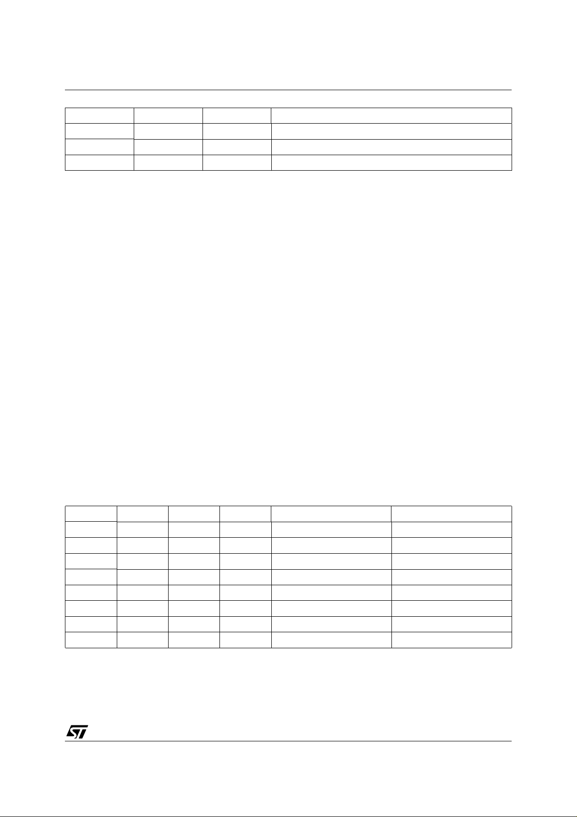
2 - BLOC DIAGRAM
MULTIWATT 15
Vdd
10
Protection
Control
Voltage Control
CBoot Vpp
13 15 14
Bootstrap
control
STV7801S
H-Clmp
LH-Tr
HL-Tr
L-Clmp
Vsslog
2
4
1
3
8
STV7801S
Timing
Control
LH Transistor
HL Transistor
DM-HLPR-FPS
DM-LH
H-Clmp
Transistor
L-Clmp
Transistor
11965
Vssp
7
12
PR
Out
3/18
STV7801S
3 - PIN DESCRIPTION
Multiwatt 15
Pin Number Pin Name Function Description
1 HL-Tr Input Power Recovery High Level/Low Level Transition
2 H-Clmp Input Main Switch High-Side Clamp Input
3 L-Clmp Input Main Switch Low-Side Clamp Input
4 LH-Tr Input Power Recovery Low Level/High Level Transition
5 PR-FPS Input Power Recovery Floating Supply
6 DM-HL Input Current Recirculation- Input Pin - High/Low Transition
7 PR Output Power Recirculation Output Stage
8 Vsslog Ground Logic Ground/Substrate Ground
9 DM-LH Output Current Recirculation- Output Pin - Low/High Transition
10 Vdd Supply Logic Supply
11 Vssp Ground Power Ground
12 Out Output Main Switch Output
13 CBoot Input Bootstrap Capacitor Input Pin
14 Vpp Supply High Voltage Supply
15 Vpp Supply High Voltage Supply
PowerSO20
Pin Number Pin Name Function Description
1 Vssub Ground Substrate Ground
2 HL-Tr Input Power Recovery High Level/Low Level Transition
3 H-Clmp Input Main Switch High-Side Clamp Input
4 L-Clmp Input Main Switch Low-Side Clamp Input
5 LH-Tr Input Power Recovery Low Level/High Level Transition
6 PR-FPS Input Power Recovery Floating Supply
7 PR-FPS Input Power Recovery Floating Supply
8
DM-HL
9 PR Output Power Recirculation Output Stage
10
11
Vssub
Vsslog
12 DM-LH Output Current Recirculation- Output Pin - Low/High Transition
13
14
15
Vdd
Vssp
Vssp
16 Out Output Main Switch Output
17 CBoot Input Bootstrap Capacitor Input Pin
Input Current Recirculation- Input Pin - High/Low Transition
Ground Substrate Ground
Ground Logic Ground/Substrate Ground
Supply Logic Supply
Ground Power Ground
Ground Power Ground
4/18
Pin Number Pin Name Function Description
18 Vpp Supply High Voltage Supply
19 Vpp Supply High Voltage Supply
20 Vssub Ground Substrate Ground
4 - CIRCUIT DESCRIPTION
STV7801S
STV7801 is a monol ithic integrated circuit implemented in ST Microelectronics BCD proprietary
technology designed as a switched power supp ly
generator for data drivers in a Plasma Display
Panel (P.D.P.) application.
The high load drive capability of STV7801 reduces
the number of devices n ecessary to drive a com plete PDP (4 to 6 devices for a 42" VGA 16/9 PDP
monitor).
STV7801 high current drive capability provides a
high power recovery efficiency coefficient superior
to 85% on constant capacitive load. The structure
of the output stage is implemented with 2 DMOS
transistors to minimise the die size. External components like bootstrap capacitor can also be implemented to increase the performances of the circuit.
STV7801 integrates level s hifters driven with 5V
CMOS compatible levels. This feature reduces the
number of discrete components such as voltage
trans lator s.
STV7801 integrates several protections like output
over-voltage, timing control and over-tem perature
to increase the reliability of the system.
Over-voltage protection consists in clamping diodes connected between Vpp, Vssp and critical
nodes of the devices.
Timing control consists in a m onitoring of the ou tput stage control signals to avoid any cross-conduction.
Over-temperature protection is activated when
junction temperature reaches the threshold values
fixed internally and sets the device in tri-state
mode.
STV7801 can drive several data drivers connected
to column electrodes of the panel. The maximum
amount of data drivers is given by the Power Recovery Current of the device and then the maximum rise/fall time of the signal. The rise and fall
time of the AC supply signal is adjusted by the value of the inductance connected to the panel capacitance through the data drivers. The amount of
STV7801 needed to gene rate the AC supply can
be reduced by increasing the rise/fall time of the
generated AC supply.
5 - CONTROL SIGN ALS TR UTH TABLE
HL-Tr LH-Tr L-Clmp H-Clmp Device Output Comments
L H L L Low to High Transition Power Saving Mode
H L L L High to Low Transition Power Saving Mode
LXLH
XLHL
X X H H Tri-State Protection Mode
XHHXTri-State Protection Mode
H X X H Tri-State Protection Mode
L L L L Tri-State Protection Mode
Vpp Power Supply Clamp
Vssp Power Ground Clamp
5/18

STV7801S
6 - POWER ON SEQUENCE
If Vpp is switched ON before Vdd, the circuit remains in Tri-State mode until Vdd reaches Vdd threshold.
If Vddis switched ON before Vpp, the circuit remains in Tri-State mode until Vpp reaches Vpp threshold.
7 - ABSOLUTE MAXIMUM RATINGS
Symbol Parameter Value Unit
Vdd Logic Supply Range -0.3,+14 V
Vpp Driver Supply Range -0.3 , + 100 V
VIn Logic Input Voltage Range -0.3, Vdd+0.3 °C
Ih-Out Main Switch High Side Current -5 A
Il-Out Main Switch Low Side Current 5 A
Ipr-Hi Power Recovery Current (note1)-7A
Ipr-Lo Power Recovery current (note1)7A
V
CBoot-Vout
Tjmax Maximum Junction Temperature (note2)
Top Operating Temperature Range -20, +70 °C
Tstg Storage Temperature Range -50, +150 °C
Difference between Boot voltage and output voltage 14 V
Internally
protected
°C
Note 1 Peak current as defined in Figure 1 on page 9
Note 2 T hese parame ters are meas ured during ST ’s internal qua lification whi ch includes tem perature ch aracterizat ion
on standard and corner batches of the process. These parameters are not tested on the parts.
Remark: ESD susceptibility
Human body Model: 100pF, 1.5kΩ
Vpp pin (14-15: Multiwatt 15) V
DM-LH pin (9: Multiwatt 15) V
By connecting a 1nF decoupling capacitor, the circuit withstands V
ESD
ESD
= 200V
=400V
=2.2kV on all pins.
ESD
8 - THERMAL DAT A
Symbol Parameter
R
th(j-a)
R
th(j-c)
Note 3 Multilayer PCB.
Note 4 Package floating in the air.
Junction - Ambient Thermal Resistance 40(note3) 35 (note4)°C/W
Junction - Case Thermal Resistance +0.6, +2.5 -0.6, +2.4
PowerSO20 MW15
Value
Unit
6/18
 Loading...