

SGS Thomson Microelectronics STV7778S Datasheet
STV7778S
DEFLECTION PROCESSOR FOR MULTISYNC MONITOR
HORIZONTAL
.
DUAL PLL CONCEP T
.
SELF-ADAPTIVE (30 TO 70kHz )
.
X-RAY PROTECTION INPUT
.
DC ADJUST AB LE DUTY-CYCLE
.
INTERNAL 1st PLL LOCK/UNLOCK IDENTIFICATION
.
WIDE RANGE DC CONTROLLED H-POSITION
.
ON/OFF S W ITCH (FOR P W R M AN A G E MENT)
.
TWO H-DRIVE POLARITIES
VERTICAL
.
VERTICAL RAMP GENERATOR
.
45 TO 120Hz AGC LO OP
.
DC CONTROLLED V-AMP, V-POS, S-AMP
AND S-CENTERING
.
ON/OFF SWITCH
B+ REGULATOR
.
INTERNAL PWM GENERATOR FOR B+
CURRENT MODE STEP-UP CONVERTER
.
DC ADJUSTABLE B+ VOLTAGE
.
OUTPUT PULSES SYNCHRONISED ON
HORIZONTAL FREQUENCY
.
INTERNAL MAX CURRENT LIMITATION
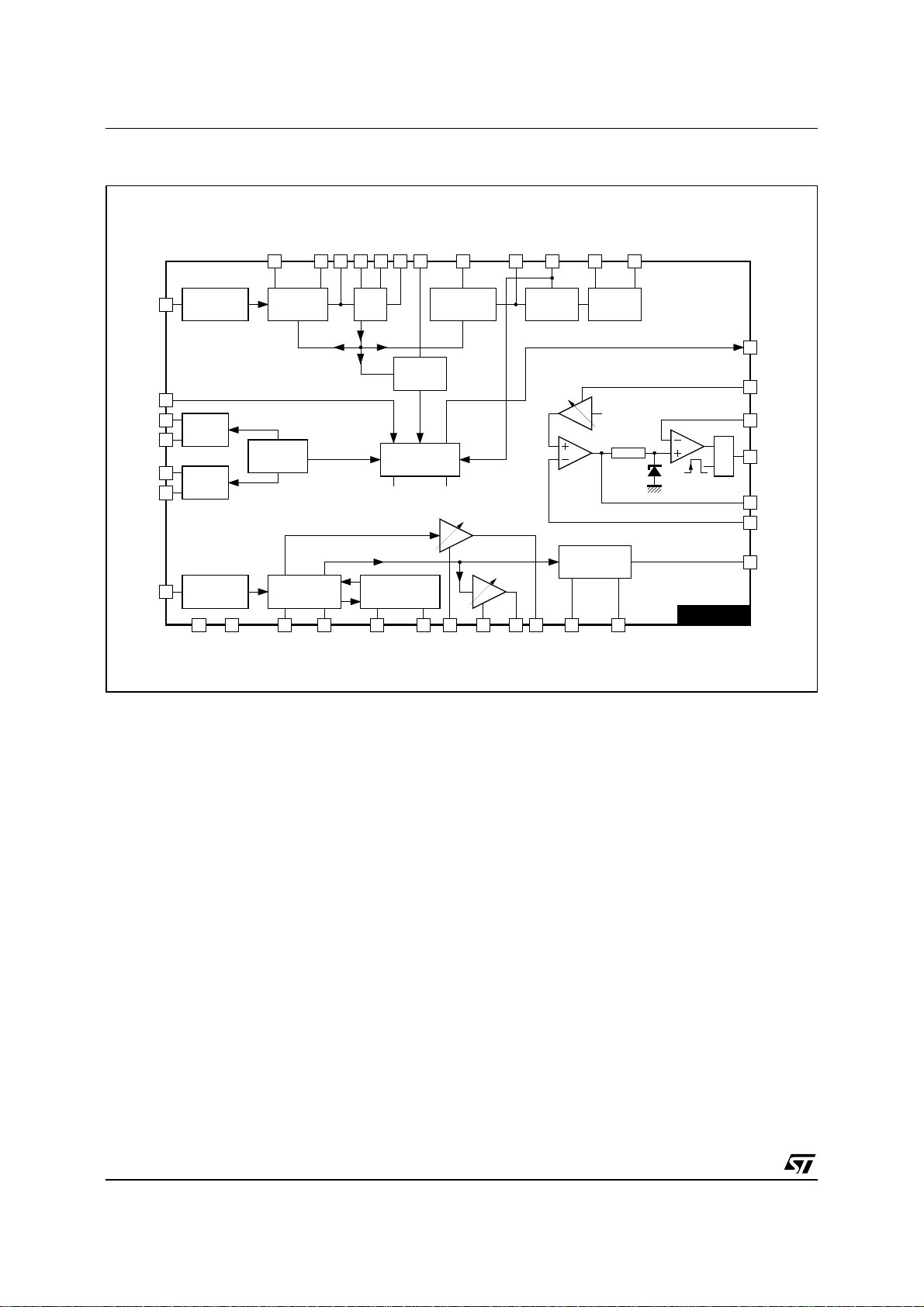
The goal of this IC is to control all the functions
related to the horizontal and vertical deflection in a
multimodes or multisync monitor.
As can be seen in the block diagram, the
STV7778S includes the following functions :
- Positive or Negative sync polarities,
- Auto-sync horizontal processing,
- H-PLL lock/unlock identification,
- Auto-sync Ver tical processing,
- East/West signal processing block,
- B+ controller,
- Safety blanking output.
An internal metal shield give to the STV7778S more
immunity against electromagnetic and electrostatic
fields, and therefore, additional safety for critical
applications (for example, in case of CRTs with
small coated area).
EWPCC
.
VERTICAL PARABOLA GENERATOR WITH DC
CONTROLLED KEYSTONE AND AMPLITUDE
GENERAL
.
COMPARED WITH THE STV7778, THE
STV7778S HAS AN INTERNAL METAL SHIELD
PROTECTION AGA INST OVER VOLTAGE.
.
POS/NEG H AND V SYNC P O L
.
SEPARATED H AND V TTL INPUT
.
SAFETY BLAN KING OUT PUT
DESCRIPTION
The STV7778S is a monolithic integrated circuit
assembled in a 42 pins shrunk dual in line plastic
package.
September 1998
SHRINK42
(Plastic Package)
ORDER CODE : STV7778S
1/11
STV7778S
PIN CONNECTIONS
PLL2C
H-DUTY
HFLY
HGND
HREF
NC
NC
NC
NC
C0
R0
PLL1F
HLOCK-CAP
FH-MIN
H-POS
XRAY-IN
HSYNC
V
GND
H-OUTEM
H-OUTCOL
1
2
3
4
5
6
7
8
9
10
11
12
13
14
15
16
17
18
CC
19
20
21 22
42 I
41
40
39
38
37
36
35
34
33
32
31
30
29
28
27
26
25
24
23
SENSE
COMP
REGIN
B+-ADJ
KEYST
E/W-AMP
E/WOUT
PLL1INHIB
VSYNC
V-POS
V
DCOUT
V-AMP
VOUT
VS-CENT
VS-AMP
VCAP
V
REF
VAGCCAP
VDND
SBLKOUT
B+OUT
7778S-01.EPS
2/11

STV7778S
PIN-OUT DESCRIPTION
Pin N° Name Function
1 PLL2C Second PLL Loop Filter
2 H-DUTY DC Control of Horizontal Drive Output Pulse Duty-cycle.
3 H-FLY Horizontal Flyback Input (Positive Polarity)
4 H-GND Horizontal Section Ground. Must be connected only to components related to H blocks.
5 H-REF Horizontal Section Reference Voltage. Must be filtered by capacitor to Pin 4
6NC
7NC
8NC
9NC
10 C0 Horizontal Oscillator Capacitor. To be connected to Pin 4.
11 R0 Horizontal Oscillator Resistor. To be connected to Pin 4.
12 PLL1F First PLL Loop Filter. To be connected to Pin 4.
13 HLOCK-CAP Firs t P L L L o ck / Un l oc k T i me C o ns tant Capacitor. Capacitor filtering the frequency change detected
14 FH-MIN
15 H-POS DC Control for Horizontal Centering
16 XRAY-IN X-RAY Protection Input (with internal latch function)
17 H-SYNC TTL Horizontal Sync Input
18 V
CC
19 GND Ground
20 H-OUTEM Horizontal Drive Output (emiter of internal transistor)
21 H-OUTCOL Horizontal Drive Output (open collector of internal transistor)
22 B+ OUT B+ PWM Regulator Output
23 SBLK OUT Safety Blanking Output. Activated duri ng frequency changes, when X-RAY input is triggere d or
24 VGND Vertical Section Signal Ground
25 VAGCCAP Memory Capacitor for Automatic Gain Control Loop in Vertical Ramp Generator
26 V
REF
27 VCAP Vertical Sawtooth Generator Capacitor
28 VS-AMP DC Control of Vertical S Shape Amplitude
29 VS-CENT DC Control of Vertical S Centering
30 VOUT Vertical Ramp Output (with frequency independant amplitude and S-correction)
31 V-AMP DC Control of Vertical Amplitude Adjustment
32 V
DCOUT
33 V-POS DC Control of Vertical Position Adjustment
34 VSYNC Vertical TTL Sync Input
35 PLL1INHIB TTL Input for PLL1 Output Current Inhibition (To be used in case of comp sync input signal)
36 E/WOUT East/West Pincushion Correction Parabola Output
37 E/W-AMP DC Control of East/West Pincushion Correction Amplitude
38 KEYST DC Control of Keystone Correction
39 B+ ADJ DC Control of B+ Adjustment
40 REGIN Regulation Input of B+ Control Loop
41 COMP B+ Error Amplifier Output for Frequency Compensation and Gain Setting
42 I
SENSE
If this pin is grounded, the horizontal and vertical outputs are inhibited. By connecting a capacitor
on this pin a soft-start function may be realized on h-drive output.
on Pin13. When frequency is changing, a blanking pulse is generated on Pin 23, the duration of this
pulse is proportionnal to the capacitor on Pin 13. To be connected to Pin 4.
DC Control for Free Running Frequency Setting. Comming from DAC output or DC voltage
generated by a resistor bridge connected between Pin 5 and 4.
Supply Voltage (12V Typical)
when VS is too low.
Vertical Section Reference Voltage
Vertical Position Reference Voltage Output Temperature Matched with V-AMP Output
Sensing of External B+ Switching Transistor Emiter Current
7778S-01.TBL
3/11
STV7778S
BLOCK DIAGRAM
PLL1INHIB
35
H-POS
PLL1FR0C0
1112 131415 21
FH-MIN
HLOCK-CAP
HFLY
10
PLL2C
1 23
H-DUTY
H-OUTEM
20
H-OUTCOL
HSYNC
XRAY-IN
HREF
HGND
VREF
VGND
VSYNC
17
16
5
4
26
24
34
INPUT
INTERFACE
H-VREF
V-VREF
INPUT
INTERFACE
1819
GND
1st PHASE
COMP
BANDGAP
VERTICAL
OSCILLATOR
27 2829 30
CC
V
VCAP
VCO
LOCK
DETECT
SAFETY
PROCESSOR
V
CC
S
CORRECTION
25 31 3233
VAGCCAP
VS-CENT
2nd PHASE
COMP
Outputs
Inhibition
V-POS
VS-AMP
V-AMP
SHAPER
VOUT
PULSE
DCOUT
V
OUTPUT
BUFFER
V
REF
EA
PARABOLA
GENERATOR
3738
KEYST
E/W-AMP
R
S
STV7778S
23
39
42
22
41
40
36
SBLKOUT
B+-ADJ
I
SENSE
B+OUT
COMP
REGIN
E/WOUT
7778S-02.EPS
4/11
 Loading...