

SGS Thomson Microelectronics STV7699 Datasheet
PLASMA DISPLAY PANEL DATA DRIVER
.
64 OUTPUTS PLASMA DISPLAY DRIVE R
.
170V ABSOLUTE MAXIMU M SUP PLY
.
5V SUPPLY FOR LOGIC
.
50/40mA SOURCE / SINK OUTPUT
.
60/60mA SOURCE / SINK OUTPUT DIODE
.
64-BIT SHIFT REGISTER (20MHz)
.
BLK, POLARITY AND H IZ CONT ROL
.
BCD TECHNOLOGY
.
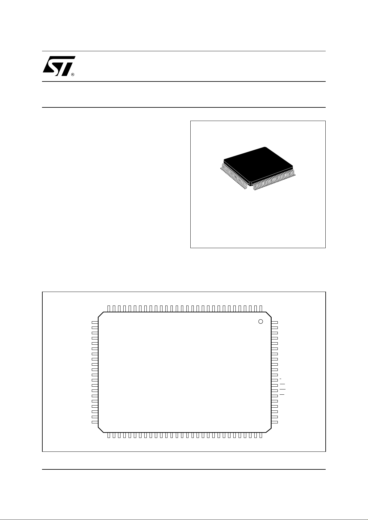
DIE or 100-PIN PQFP PACKAGE
DESCRIPTION
The STV7699 is a Plasma Display Panel (PDP)
data driver implemented in ST’s proprietary BCD
technology. Using a 4-bit wide cascadable shift
register, it drives 64 high current & high voltage outputs. By s erialy connecting s everal STV7699, any horizontal pixel definition can be performed. The 20MHz
shift clock gives an equivalent 80MHz shift register.
The STV7699 is supplied with a separated 170V
power out put s upply and a 5V logic supply.
STV7699
PRODUCT PREVIEW
PQFP100 (14 x 20 x 2.80mm)
(Full Plastic Quad Flat Pack)
ORDER CODE : STV7699
All command inputs are CMOS compatible.
The STV 7699 pack age is a 1 00-pin PQF P. It is als o
available as die.
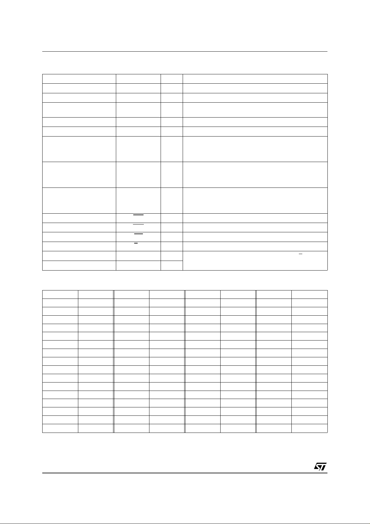
PIN CONNECTIONS
SSP
V
OUT4
OUT5
OUT6
OUT7
987654321
SSP
V
OUT58
OUT59
OUT60
OUT61
OUT25
OUT26
OUT27
OUT28
V
OUT29
OUT30
OUT31
OUT32
V
V
SSSUB
OUT33
OUT34
OUT35
OUT36
V
OUT37
OUT38
OUT39
OUT40
PP
VPPV
OUT24
302928272625242322212019181716151413121110
31
32
33
34
35
SSP
36
37
38
39
40
SSP
41
42
43
44
45
46
SSP
47
48
49
50
5152535455565758596061626364656667686970717273747576777879
PP
VPPV
OUT41
SSP
V
OUT20
OUT22
OUT23
OUT21
OUT16
OUT17
OUT18
OUT19
STV7699
PQFP100
(Top View)
SSP
V
OUT42
OUT43
OUT44
OUT45
OUT46
OUT47
OUT48
OUT49
SSP
V
OUT12
OUT13
OUT14
OUT15
SSP
V
OUT50
OUT51
OUT52
OUT53
OUT8
OUT9
OUT10
OUT11
OUT54
OUT55
OUT56
OUT57
January 1999
This is advance information on a new product now in development or undergoing evaluation. Details are subject to change without notice.
PP
V
OUT1
OUT2
OUT3
100
99
98
97
96
95
94
93
92
91
90
89
88
87
86
85
84
83
82
81
80
PP
V
OUT62
OUT63
OUT64
V
A1
A2
A3
A4
CLK
STB
V
V
V
V
F/R
BLK
POL
HIZ
B4
B3
B2
B1
V
CC
SSLOG
SSLOG
SSLOG
SSLOG
SSSUB
7699-01.EPS
1/9
STV7699
PIN ASSIGNMENT
(PQFP100)
Pin Number Symbol Type Function
100 V
1 - 29 - 30 - 51 - 52 - 80 V
6 - 15 - 24 - 35 - 40
46 - 57 - 66 - 75
90 to 93 V
41 - 81 V
2 to 5 - 7 to 14 - 16 to 23
25 to 28 - 31 to 34 - 36 to 39
42 to 45 - 47 to 50 - 53 to 56
58 to 65 - 67 to 74 - 76 to 79
95 CLK Input Clock of data shift register
94 STB Input Latch of data to outputs
88
87
86 HIZ Input Power Output High Impedance Control
89 F/R Input Selection of shift direction
96 to 99 A4 to A1 Input
82 to 85 B1 to B4 Output
CC
PP
V
SSP
SSLOG
SSSUB
Supply 5V Logic Supply
Supply High Voltage Supply of power outputs
Ground Ground of power outputs
Ground Logic Ground
Ground Substrate Ground
OUT1 to OUT 64 Output Power Output
Low to High transition makes the data enter into the shift
register and available at the output stage and at the output
of the shift register.
When the STB signal is set to low level, data are transferred
into the latch stage. When STB is set at high level, data are
held in the latch stage.
BLK Input Power Output Blanking Control
POL Input Power Output Polarity Control
Shift register data input and output according to
When set to low, Ai = input and Bi = output.
F/R value.
7699-01.TBL
PIN ASSIGNMENT
(Power Outputs)
Output N° Pin N° Output N° Pin N° Output N° Pin N° Output N° Pin N°
1 2 17 20 33 42 49 62
2 3 18 21 34 43 50 63
3 4 19 22 35 44 51 64
4 5 20 23 36 45 52 65
5 7 21 25 37 47 53 67
6 8 22 26 38 48 54 68
7 9 23 27 39 48 55 69
8 10242840505670
9 11253141535771
10 12 26 32 42 54 58 72
11 13 27 33 43 55 59 73
12 14 28 34 44 56 60 74
13 16 29 36 45 58 61 76
14 17 30 37 46 59 62 77
15 18 31 38 47 60 63 78
16 19 32 39 48 61 64 79
7699-02.TBL
2/9

STV7699
PAD DIMENSIONS
(in µm)
The reference is the center of the die (x = 0, y = 0).
LEFT SIDE from top to bottom
Name Center : X Center : Y Size : x Size : y
V
PP
OUT1 -1738.0 2703.0 90.0 75.0
OUT2 -1738.0 2570.5 90.0 75.0
OUT3 -1738.0 2411.0 90.0 75.0
OUT4 -1738.0 2228.5 90.0 75.0
V
SSP
OUT5 -1738.0 1952.0 90.0 75.0
OUT6 -1738.0 1813.5 90.0 75.0
OUT7 -1738.0 1631.0 90.0 75.0
OUT8 -1738.0 1453.0 90.0 75.0
OUT9 -1738.0 1235.5 90.0 75.0
OUT10 -1738.0 1046.5 90.0 75.0
OUT11 -1738.0 862.0 90.0 75.0
OUT12 -1738.0 712.5 90.0 75.0
V
SSP
OUT13 -1738.0 431.0 90.0 75.0
OUT14 -1738.0 293.0 90.0 75.0
OUT15 -1738.0 82.5 90.0 75.0
OUT16 -1738.0 -109.5 90.0 75.0
OUT17 -1738.0 -277.0 90.0 75.0
OUT18 -1738.0 -471.0 90.0 75.0
OUT19 -1738.0 -691.5 90.0 75.0
OUT20 -1738.0 -822.5 90.0 75.0
V
SSP
OUT21 -1738.0 -1096.0 90.0 75.0
OUT22 -1738.0 -1335.5 90.0 75.0
OUT23 -1738.0 -1569.0 90.0 75.0
OUT24 -1738.0 -1697.5 90.0 75.0
V
PP
-1738.0 2867.5 90.0 75.0
-1738.0 2093.0 90.0 75.0
-1738.0 566.0 90.0 75.0
-1738.0 -953.0 90.0 75.0
-1715.0 -2045.0 90.0 200.0
Right SIDE from bottom to top
Name Center : X Center : Y Size : x Size : y
V
PP
OUT41 1737.5 -1646.0 90.0 75.0
OUT42 1737.5 -1507.0 90.0 75.0
OUT43 1737.5 -1328.0 90.0 75.0
OUT44 1737.5 -1096.0 90.0 75.0
V
SSP
OUT45 1737.5 -822.5 90.0 75.0
OUT46 1737.5 -691.5 90.0 75.0
OUT47 1737.5 -471.0 90.0 75.0
OUT48 1737.5 -277.0 90.0 75.0
OUT49 1737.5 -109.5 90.0 75.0
OUT50 1737.5 82.5 90.0 75.0
OUT51 1737.5 293.0 90.0 75.0
OUT52 1737.5 431.0 90.0 75.0
VSSP 1737.5 566.0 90.0 75.0
OUT53 1737.5 712.5 90.0 75.0
OUT54 1737.5 862.0 90.0 75.0
OUT55 1737.5 1046.5 90.0 75.0
OUT56 1737.5 1235.5 90.0 75.0
OUT57 1737.5 1453.0 90.0 75.0
OUT58 1737.5 1631.0 90.0 75.0
OUT59 1737.5 1813.5 90.0 75.0
OUT60 1737.5 1952.0 90.0 75.0
V
SSP
OUT61 1737.5 2228.5 90.0 75.0
OUT62 1737.5 2411.0 90.0 75.0
OUT63 1737.5 2570.5 90.0 75.0
OUT64 1737.5 2703.0 90.0 75.0
V
PP
1600.5 -2087.0 90.0 200.0
1737.5 -953.0 90.0 75.0
1737.5 2093.0 90.0 75.0
1737.5 2873.5 90.0 75.0
BOTTOM SIDE from left to right
Name Center : X Center : Y Size : x Size : y
OUT25 -1443.5 -3077.0 75.0 90.0
OUT26 -1249.0 -3077.0 75.0 90.0
OUT27 -1049.5 -3077.0 75.0 90.0
OUT28 -889.0 -3077.0 5.0 90.0
V
SSP
OUT29 -614.0 -3077.0 75.0 90.0
OUT30 -467.5 -3077.0 75.0 90.0
OUT31 -332.0 -3077.0 75.0 90.0
OUT32 -186.5 -3077.0 75.0 90.0
V
SSP
V
SSSUB
OUT33 209.5 -3077.0 75.0 90.0
OUT34 342.5 -3077.0 75.0 90.0
OUT35 467.5 -3077.0 75.0 90.0
OUT36 607.5 -3077.0 75.0 90.0
V
SSP
OUT37 892.5 -3077.0 75.0 90.0
OUT38 1045.5 -3077.0 75.0 90.0
OUT39 1252.0 -3077.0 75.0 90.0
OUT40 1433.5 -3077.0 75.0 90.0
-753.0 -3077.0 75.0 90.0
-54.0 -3077.0 75.0 90.0
78.0 -3077.0 75.0 90.0
752.0 -3077.0 75.0 90.0
TOP SIDE from right to left
Name Center : X Center : Y Size : x Size : y
V
SSSUB
B1 1478.5 3073.5 75.0 90.0
B2 1228.5 3077.0 75.0 90.0
B3 978.5 3077.0 75.0 90.0
B4 847.5 3077.0 75.0 90.0
HIZ 716.5 3077.0 75.0 90.0
POL 486.5 3077.0 75.0 90.0
BLK 355.5 3077.0 75.0 90.0
F/R 224.5 3077.0 75.0 90.0
V
SSLOG
V
SSLOG
STB -582.0 3077.0 75.0 90.0
CLK -713.0 3077.0 75.0 90.0
A4 -844.0 3077.0 75.0 90.0
A3 -975.0 3077.0 75.0 90.0
A2 -1106.0 3077.0 75.0 90.0
A1 -1471.5 3077.0 75.0 90.0
V
CC
1628.5 3073.5 75.0 90.0
31.0 3077.0 200.0 90.0
-354.5 3077.0 200.0 90.0
-1629.0 3077.0 75.0 90.0
3/9
 Loading...