

SGS Thomson Microelectronics STV7697A Datasheet
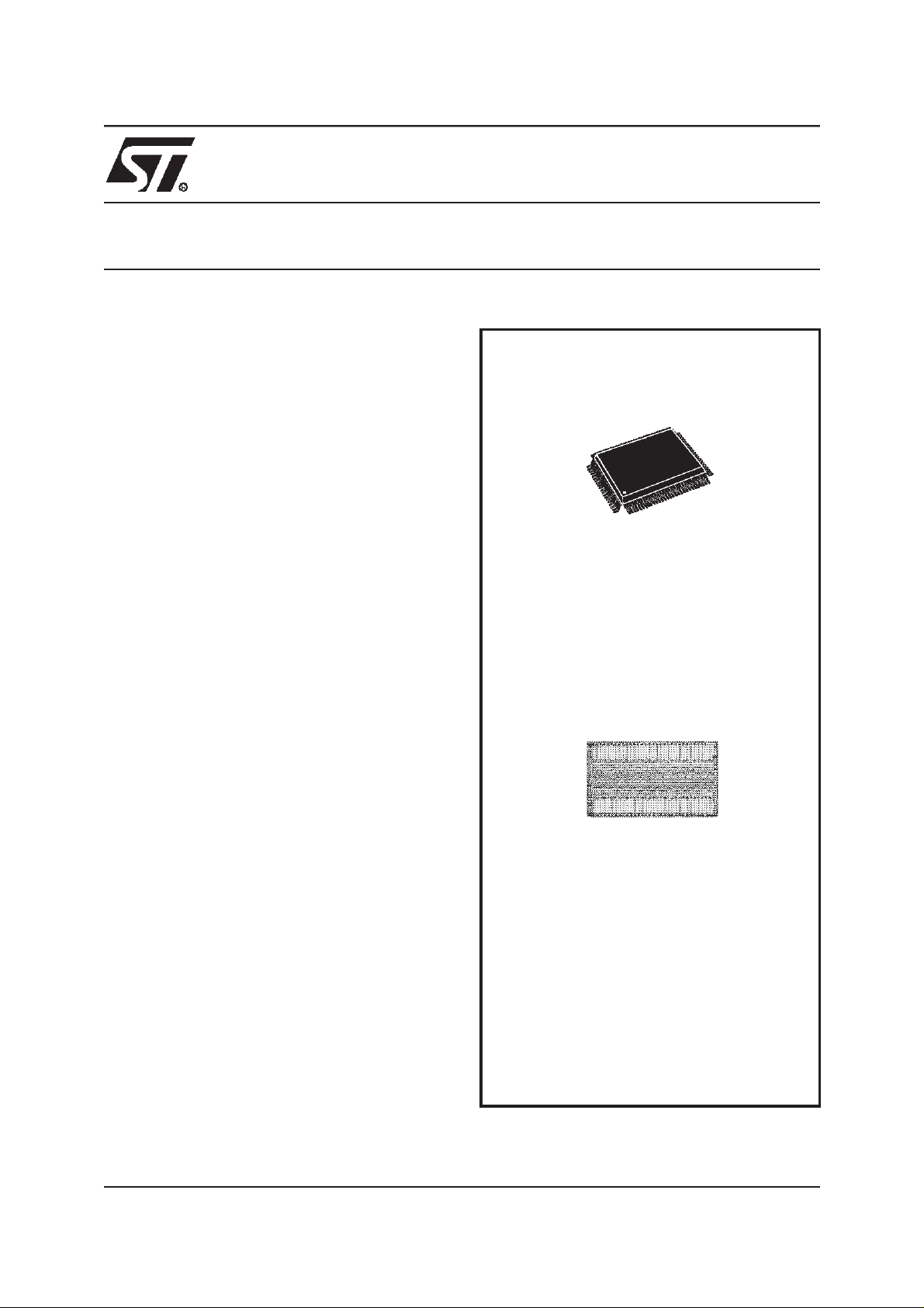
STV7697A
PLASMA DISPLAY PANEL SCAN DRIVER
FEATURES
■ 64 OUTPUTS PLASMA DISPLAY DRIVER
■ 170V ABSOLUTE MAXIMUM SUPPLY
■ 5V SUPPLY FOR LOGIC
■ 100/400 mA SOURCE / SINK OUTPUT
■ 700 mA SOURCE / SINK OUTPUT DIODE
■ 64-BIT SHIFT REGISTER (20 MHz)
■ BLANK CONTROL
■ COMPLEMENTARY OUTPUT CONTROL
■ BCD TECHNOLOGY
■ 100 PINS PQFP PACKAGE OR DICE.
DESCRIPTION
The STV7697A is a scan driver for Plasma
Display Panel (PDP) implemented in ST’s
proprietary BCD technology. Using a 64-bit
cascadable 20 MHz shift register, it drives 64 high
current & high voltage outputs. By serially
connecting several STV7697A, any vertical pixel
definition can be performed. The STV7697A is
supplied with a separated 160V power output
supply and a 5V logic supply.All command inputs
are CMOS compatible.
The STV769 7A package is a 100 pins PQFP.
.
PQFP100 (14 x 20 x 2.80 mm)
(Full Plastic Quad Flat Pack)
ORDER CODE: STV7697A
ORDER CODE: STV7697A/WAF (1)
(1): Unsawn Tested Wafer
Version 4.2
June 2000 1/15
This ispreliminary information on a new product indevelopment orundergoing evaluation. Details are subject tochange without notice.
1

TABLE OF CONTENTS
PIN ASSIGNMENT . ............................................................ 4
BLOCK DIAGRAM . ............................................................ 7
CIRCUIT DESCRIPTION . . . . . . . . . ................................................ 7
Note 1 ABSOLUTE MAXIMUM RATINGS . . . . . . . . . . . . ............................... 8
Note 1 THERMAL DATA . . . . . . . . . ................................................ 8
Note 5 ELECTRICAL CHARACTERISTICS .......................................... 9
Note 6 AC TIMINGS REQUIREMENTS . . . . . . . . . . . . . . . . . . . . . . . . . . . . . . . . . . . . . . . . . . . . . 10
Note 6 AC TIMINGS CHARACTERISTICS . . . . . . . . . ................................. 10
Figure 2. INPUT/OUTPUT SCHEMATICS . . . . . . . . . . ................................. 13
Figure 6. PACKAGE MECHANICAL DATA . . . . . . . .................................. 14
2/15
2
2
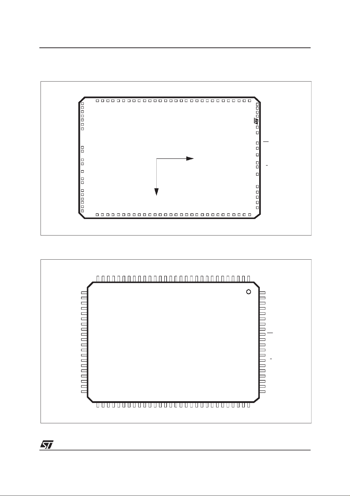
PIN CONNECTIONS
(Die pinout)
OUT36
OUT35
OUT38
OUT37
OUT40
OUT39
OUT42
OUT41
OUT43
OUT44
OUT46
OUT45
OUT48
OUT47
OUT50
OUT49
OUT52
OUT51
OUT53
OUT54
OUT56
OUT55
OUT58
OUT57
OUT60
OUT59
OUT62
OUT61
OUT64
OUT63
STV7697A
OUT34
OUT33
V
PP
V
SSP
V
SSP
V
SSP
V
PP
V
SSSUB
V
SSLOG
V
SSLOG
V
CC
V
SSLOG
V
SSSUB
V
PP
V
SSP
V
SSP
V
SSP
V
PP
OUT32
OUT31
PIN CONNECTIONS
(TQFP pinout)
OUT30
OUT29
OUT35
OUT28
OUT37
OUT36
OUT27
OUT26
OUT38
OUT25
OUT40
OUT39
STV7697A
Bare Die
(0,0)
x
OUT24
OUT23
OUT22
OUT21
OUT20
OUT19
OUT18
OUT47
OUT46
OUT45
OUT43
OUT42
OUT41
OUT44
OUT17
OUT16
OUT49
OUT48
OUT15
OUT14
OUT51
OUT50
y
OUT13
OUT12
OUT53
OUT52
OUT11
OUT10
OUT55
OUT54
OUT9
OUT57
OUT56
OUT8
OUT7
OUT59
OUT58
OUT6
OUT5
OUT61
OUT60
OUT4
OUT3
OUT63
OUT62
OUT2
OUT1
V
P
P
V
SSP
V
SSP
V
PP
V
SSLOG
CLK
STB
SOUT(SIN)
V
CC
SIN(SOUT)
F/R
BLK
POL
V
PP
V
SSP
V
SSP
V
PP
OUT34
OUT33
V
V
V
V
SSSUB
V
SSLOG
V
SSLOG
V
SSLOG
V
SSSUB
V
V
V
OUT32
OUT31
302928272625242322212019181716151413121110
31
32
33
V
PP
34
SSP
35
SSP
36
SSP
37
V
PP
38
39
40
V
CC
41
42
43
44
V
PP
45
SSP
46
SSP
47
SSP
V
48
PP
49
STV7697A
PQFP100
50
5152535455565758596061626364656667686970717273747576777879
OUT30
OUT29
OUT28
OUT27
OUT26
OUT25
OUT24
OUT23
OUT22
OUT21
OUT20
OUT19
OUT18
OUT17
OUT16
OUT15
OUT14
OUT13
987654321
OUT9
OUT11
OUT10
OUT8
OUT12
OUT7
OUT6
OUT5
OUT4
OUT3
OUT2
100
99
98
97
96
95
94
93
92
91
90
89
88
87
86
85
84
83
82
81
80 OUT64
OUT1
V
PP
V
SSP
V
SSP
V
PP
NC
NC
V
SSLOG
CLK
STB
SOUT(SIN)
V
CC
SIN(SOUT)
NC
F/R
BLK
POL
V
PP
V
SSP
V
SSP
V
PP
3/15
3
STV7697A
PIN ASSIGNMENT
(TQFP100)
Pin Number Symbol Type Function
33-37-44-48-81-84-97-100 V
41 - 90 V
34-35-36-45-46-47-82-83-98-99 V
38-43 V
39-40-42-94 V
1 to 32, 49 to 80 OUT 64 to OUT 1 Output Power Output
91 SOUT (SIN) Output Shift Register Data Output (forward)
85 POL Input Polarity Selection
86 BLK Input Output Blanking Command
87 F/ Input Selection of shift direction
89 SIN (SOUT) Input Shift Register Data Input (forward)
92 Input Latch of data to outputs
93 CLK Input Clock of data shift register
88-95-96 NC -
PP
CC
SSP
SSSUB
SSLOG
R
STB
Supply High Voltage Supply of power outputs
Supply 5 V Logic Supply
Ground Ground of power outputs
Ground Substrate Ground
Ground Logic Ground
PIN ASSIGNMENT (Power Outputs)
Output N° Pin N°
180 1764 3332 4916
279 1863 3431 5015
378 1962 3530 5114
477 2061 3629 5213
576 2160 3728 5312
675 2259 3827 5411
774 2358 3926 5510
8 73 2457 4025 569
9 72 2556 4124 578
10 71 26 55 42 23 58 7
11 70 27 54 43 22 59 6
12 69 28 53 44 21 60 5
13 68 29 52 45 20 61 4
14 67 30 51 46 19 62 3
15 66 31 50 47 18 63 2
16 65 32 49 48 17 64 1
Output N° Pin N° Output N° Pin N° Output N° Pin N°
4/15
3
PADSDIMENSIONS (in µm)/ PADS POSITIONS
The reference is the centre of the die (x=0, y=0)
TOP SIDE from left to right
Name Centre:X Centre:Y Size:x SIze: y
V
V
V
V
V
SSLOG
SSP
SSP
-2468.5 4135.0 75.0 90.0
PP
-2313.5 4135.0 75.0 90.0
-2188.5 4135.0 75.0 90.0
-2063.5 4134.5 75.0 90.0
PP
-1620.0 4135.0 75.0 90.0
CLK -1430.0 4135.0 75.0 90.0
STB -781.0 4135.0 75.0 90.0
SOUT -612.5 4135.0 75.0 90.0
V
CC
-335.5 4144.5 75.0 90.0
SIN 379.5 4135.0 75.0 90.0
F/R 548.0 4135.0 75.0 90.0
BLK 1082.0 4135.0 75.0 90.0
POL 1853.0 4135.0 75.0 90.0
2021.5 4140.0 75.0 90.0
2156.5 4140.0 75.0 90.0
2291.5 4140.0 75.0 90.0
2454.5 4129.5 75.0 90.0
V
V
V
V
PP
SSP
SSP
PP
BOTTOM SIDE from left to right
Name Centre:X Centre:Y Size:x SIze: y
OUT34 -2468.0 -4087.5 75.0 90.0
OUT33 -2318.0 -4089.5 75.0 90.0
V
V
V
V
V
V
SSSUB
V
SSLOG
V
SSLOG
V
V
SSLOG
V
SSSUB
SSP
SSP
SSP
CC
-2182.0 -4089.5 75.0 90.0
PP
-2047.0 -4093.0 75.0 90.0
-1912.0 -4093.0 75.0 90.0
-1777.0 -4093.0 75.0 90.0
-1642.0 -4089.5 75.0 90.0
PP
-683.0 -4088.0 75.0 90.0
-382.5 -4088.0 75.0 90.0
419.5 -4087.5 75.0 90.0
618.5 -4087.5 75.0 90.0
951.0 -4087.5 75.0 90.0
1308.0 -4087.5 75.0 90.0
STV7697A
BOTTOM SIDE from left to right (continued)
Name Centre:X Centre:Y Size:x SIze: y
V
PP
V
SSP
V
SSP
V
SSP
V
PP
OUT32 2318.0 -4093.5 75.0 90.0
OUT31 2468.5 -4093.5 75.0 90.0
RIGHT SIDE from top to bottom
Name Centre:X Centre:Y Size:x SIze: y
OUT1 2647.0 3697.0 90.0 75.0
OUT2 2647.0 3484.0 90.0 75.0
OUT3 2647.0 3238.5 90.0 75.0
OUT4 2647.0 2992.5 90.0 75.0
OUT5 2647.0 2743.0 90.0 75.0
OUT6 2647.0 2506.5 90.0 75.0
OUT7 2647.0 2264.0 90.0 75.0
OUT8 2647.0 2018.0 90.0 75.0
OUT9 2647.0 1774.5 90.0 75.0
OUT10 2647.0 1529.0 90.0 75.0
OUT11 2647.0 1285.5 90.0 75.0
OUT12 2647.0 1040.0 90.0 75.0
OUT13 2647.0 796.5 90.0 75.0
OUT14 2647.0 551.0 90.0 75.0
OUT15 2647.0 307.5 90.0 75.0
OUT16 2647.0 62.0 90.0 75.0
OUT17 2647.0 -181.5 90.0 75.0
OUT18 2647.0 -427.0 90.0 75.0
OUT19 2647.0 -670.5 90.0 75.0
OUT20 2647.0 -916.0 90.0 75.0
OUT21 2647.0 -1159.5 90.0 75.0
OUT22 2647.0 -1405.0 90.0 75.0
OUT23 2647.0 -1648.5 90.0 75.0
OUT24 2647.0 -1894.0 90.0 75.0
1438.5 -4087.5 75.0 90.0
1797.5 -4093.5 75.0 90.0
1932.5 -4093.5 75.0 90.0
2067.5 -4093.5 75.0 90.0
2193.0 -4093.5 75.0 90.0
5/15
3
 Loading...