

SGS Thomson Microelectronics STV7617DU Datasheet
This ispreliminary information on a new product indevelopment orundergoing evaluation. Details are subject tochange without notice.
Version 4.1
June 2000 1/17
STV7617, STV7617D, STV7617U
PLASMA DISPLAYPANEL SCAN DRIVER
FEATURE
■ 64/65 SELECTABLE OUTPUT PLASMA
DISPLAY DRIVER
■ 100 V ABSOLUTE MAXIMUM SUPPLY
■ 5 V SUPPLY FOR LOGIC
■ 100/850 mA SOURCE/SINK OUTPUT
■ 700 mA SOURCE/SINK OUTPUT DIODE
■ 65-bit BIDIRECTIONAL SHIFT REGISTER
(8 MHz)
■ HIGH IMPEDANCE OUTPUT CONTROL
■ BCD TECHNOLOGY
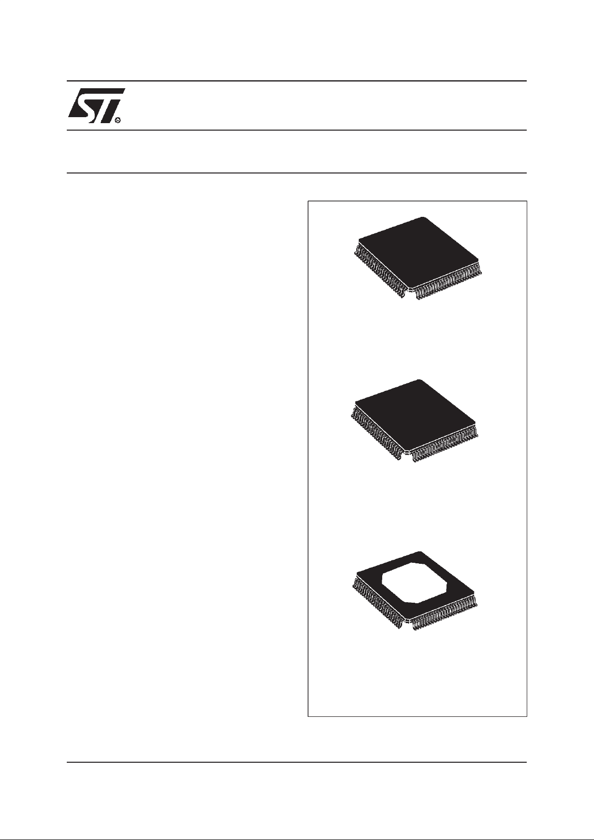
■ 100-PIN TQFP PACKAGE WITH
INTEGRATED HEATSINK
DESCRIPTION
The STV7617 is a scan driver for Plasma Display
Panel (PDP) implemented in ST’s proprietary
BCD technology. Using a 65-bit cascadable
8 MHz shift register, it drives 65 high current &
high voltage outputs.The STV7617 can beconfigured either in 64 or 65 outputs depending on the
SEL input Pin.
By serially connecting several STV7617, any vertical pixel definition can be performed. The
STV7617 is supplied with a separated 90V power
output supply and a 5 V logic supply. All command
inputs are CMOS compatible. The STV7617 package is a 100-pin TQFP with integrated heatsink located on the bottom (STV7617D) or top
(STV7617U) of the package. It is also available
without heatsink (STV7617).
TQFP100 (14 x 14 x 1.4 mm Slug-down)
(Thin Plastic Quad Flat Pack)
ORDER CODE: STV7617D
TQFP100 (14 x 14 x 1.4 mm Slug-up)
(Thin Plastic Quad Flat Pack)
ORDER CODE: STV7617U
TQFP100 (14 x 14 x 1.4 mm)
(Thin Plastic Quad Flat Pack)
ORDER CODE: STV7617
1

TABLE OF CONTENTS
2
2/17
PIN CONNECTIONS (SLUG-UP) . . . . . . . ............................................3
PIN CONNECTIONS (SLUG-DOWN) . . . ............................................ 4
PIN CONNECTIONS (NO SLUG) . . . ................................................ 5
PIN ASSIGNMENT . . . . . . . . . . . . . . . . . . . . . ......................................... 6
BLOCK DIAGRAM .............................................................. 7
CIRCUIT DESCRIPTION . . . . . . . . . . . . . . . . . . . . . . . .................................. 7
ABSOLUTE MAXIMUM RATINGS ................................................. 8
THERMAL DATA . . . . . . . . . . . . . . . ................................................ 8
ELECTRICAL CHARACTERISTICS . . . . . . . . . . . . . ...................................9
AC TIMING REQUIREMENTS . . . . . . . . . . . . . . . . . . . . . . . . . ........................... 10
AC TIMING CHARACTERISTICS . . . . . . ........................................... 10
INPUT/OUTPUT CHARACTERISTICS . . . . . . . . . . . . . . . . . . . . . . . . . . . . . . . . . . . . . . . . . . . . . 13
PACKAGE MECHANICAL DATA (SLUG-DOWN) . . . . . . . . . . . . . . . . . . . . . . . . . . . . ........ 14
PACKAGE MECHANICAL DATA (SLUG-UP) . . . . . . . . . . . . . . . . . . . . . . . . . . . . ...........15
PACKAGE MECHANICAL DATA (NO SLUG) . . . .................................... 16
2

STV7617, STV7617D, STV7617U
3/17
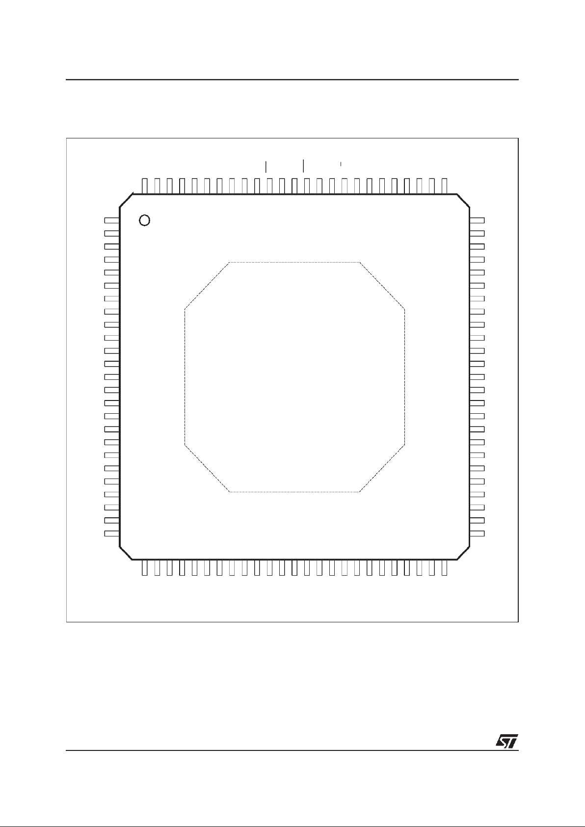
PIN CONNECTIONS (SLUG-UP)
(TQFP100 Slug-up)
1
2
3
4
5
6
7
8
9
10
11
12
13
14
15
16
17
18
19
20
21
22
23
24
25
75
74
73
72
71
70
69
68
67
66
65
64
63
62
61
60
59
58
57
56
55
54
53
52
51
26272829303132333435363738394041424344454647484950
100
9998979695949392919089888786858483828180797877
76
OUT63
OUT62
OUT61
OUT60
OUT59
OUT58
OUT57
OUT56
OUT55
OUT54
OUT33
OUT52
OUT51
OUT50
OUT49
OUT48
OUT47
OUT46
OUT45
OUT44
OUT43
OUT42
OUT41
OUT40
OUT39
OUT3
OUT4
OUT5
OUT6
OUT7
OUT8
OUT9
OUT10
OUT11
OUT12
OUT13
OUT14
OUT15
OUT16
OUT17
OUT18
OUT19
OUT20
OUT21
OUT22
OUT23
OUT24
OUT25
OUT26
OUT27
OUT28
OUT29
OUT30
NC
V
SSPVSSP
V
SSP
NC
VPPV
PP
OUT31
OUT32
OUT33
OUT34
OUT35
VPPVPPNC
V
SSSUB
V
SSPVSSP
NC
OUT36
OUT37
OUT38 OUT64
OUT65
VPPVPPNC
V
SSP
V
SSP
V
SSLOG
F/R
SOUT
CLK
STB
VCCBLK
HIZ
SIN
SEL
V
SSLOG
V
SSP
V
SSP
NC
VPPV
PP
OUT1
OUT2
STV7617U
TQFP100
(Top View)
3
STV7617, STV7617D, STV7617U
4/17
PIN CONNECTIONS (SLUG-DOWN)
(TQFP100 Slug-down)
1
2
3
4
5
6
7
8
9
10
11
12
13
14
15
16
17
18
19
20
21
22
23
24
25
75
74
73
72
71
70
69
68
67
66
65
64
63
62
61
60
59
58
57
56
55
54
53
52
51
26272829303132333435363738394041424344454647484950
100
9998979695949392919089888786858483828180797877
76
OUT63
OUT62
OUT61
OUT60
OUT59
OUT58
OUT57
OUT56
OUT55
OUT54
OUT33
OUT52
OUT51
OUT50
OUT49
OUT48
OUT47
OUT46
OUT45
OUT44
OUT43
OUT42
OUT41
OUT40
OUT39
OUT3
OUT4
OUT5
OUT6
OUT7
OUT8
OUT9
OUT10
OUT11
OUT12
OUT13
OUT14
OUT15
OUT16
OUT17
OUT18
OUT19
OUT20
OUT21
OUT22
OUT23
OUT24
OUT25
OUT26
OUT27
OUT28
OUT29
OUT30
NC
V
SSPVSSPVSSP
NC
VPPV
PP
OUT31
OUT32
OUT33
OUT34
OUT35
V
PPVPP
NC
V
SSSUB
V
SSPVSSP
NC
OUT36
OUT37
OUT38 OUT64
OUT65
V
PPVPP
NC
V
SSP
V
SSP
V
SSLOG
F/R
SOUT
CLK
STB
VCCBLK
HIZ
SIN
SEL
V
SSLOG
V
SSP
V
SSP
NC
VPPVPPOUT1
OUT2
STV7617D
TQFP100
(Top View)
3
STV7617, STV7617D, STV7617U
5/17
PIN CONNECTIONS (NO SLUG)
(TQFP100)
1
2
3
4
5
6
7
8
9
10
11
12
13
14
15
16
17
18
19
20
21
22
23
24
25
75
74
73
72
71
70
69
68
67
66
65
64
63
62
61
60
59
58
57
56
55
54
53
52
51
26272829303132333435363738394041424344454647484950
100
9998979695949392919089888786858483828180797877
76
OUT63
OUT62
OUT61
OUT60
OUT59
OUT58
OUT57
OUT56
OUT55
OUT54
OUT33
OUT52
OUT51
OUT50
OUT49
OUT48
OUT47
OUT46
OUT45
OUT44
OUT43
OUT42
OUT41
OUT40
OUT39
OUT3
OUT4
OUT5
OUT6
OUT7
OUT8
OUT9
OUT10
OUT11
OUT12
OUT13
OUT14
OUT15
OUT16
OUT17
OUT18
OUT19
OUT20
OUT21
OUT22
OUT23
OUT24
OUT25
OUT26
OUT27
OUT28
OUT29
OUT30
NC
V
SSPVSSPVSSP
NC
VPPV
PP
OUT31
OUT32
OUT33
OUT34
OUT35
VPPVPPNC
V
SSSUB
V
SSPVSSP
NC
OUT36
OUT37
OUT38 OUT64
OUT65
VPPVPPNC
V
SSP
V
SSP
V
SSLOG
F/R
SOUT
CLK
STB
VCCBLK
HIZ
SIN
SEL
V
SSLOG
V
SSP
V
SSP
NC
VPPVPPOUT1
OUT2
TQFP100
(Top View)
STV7617
3

STV7617, STV7617D, STV7617U
6/17
PIN ASSIGNMENT
(TQFP100)
PIN ASSIGNMENT (Power Outputs)
Pin Number
Symbol Type Function
TQFP100 Slug-up
TQFP100 Slug-down/
TQFP100 No slug
88 88 V
CC
Supply 5 V Logic Supply
34-35-41-42
78-79-97-98
34-35-41-42
78-79-97-98
V
PP
Supply High Voltage Supply of power outputs
30-31-44-45
46-81-82-94-95
30-31-32-45
46-81-82-94-95
V
SSP
Ground Ground of power outputs
83-93 83-93 V
SSLOG
Ground Logic Ground
32 44 V
SSSUB
Ground Substrate Ground
77 to 48, 40 to 36,
28 to 1, 100-99
99-100, 1 to 28,
36 to 40,48 to 77
OUT1 to OUT65 Output Power Output
91 85 SOUT (SIN) Output Shift Register Data Output
90 86 CLK Input Clock of data shift register
89 87 Input Latch of data to outputs
87 89 BLK Input Power Output Blanking Control
86 90 Input Power Output High Impedance Control
85 91 SIN (SOUT) Input Shift Register Data Input
84 92 SEL Input Selection of number of power outputs
92 84 F/ Input Selection of shift direction
29-33-43-47-80-96 29-33-43-47-80-96 NC - Not connected
STB
HIZ
R
Output
Number
Pin Number
Output
Number
Pin Number
Output
Number
Pin Number
Slug-down/
No slug
Slug-up
Slug-down/
No slug
Slug-up
Slug-down/
No slug
Slug-up
1 7799 235521 451957
2 76 100 24 54 22 46 18 58
3 75 1 25 53 23 47 17 59
4 74 2 26 52 24 48 16 60
5 73 3 27 51 25 49 15 61
6 72 4 28 50 26 50 14 62
7 71 5 29 49 27 51 13 63
8 70 6 30 48 28 52 12 64
9 69 7 31 40 36 53 11 65
10 68 8 32 39 37 54 10 66
11 67 9 33 38 38 55 9 67
12 66 10 34 37 39 56 8 68
13 65 11 35 36 40 57 7 69
14 64 12 36 28 48 58 6 70
15 63 13 37 27 49 59 5 71
16 62 14 38 26 50 60 4 72
17 61 15 39 25 51 61 3 73
18 60 18 40 24 52 62 2 74
19 59 17 41 23 53 63 1 75
20 58 18 42 22 54 64 100 76
21 57 19 43 21 55 65 99 77
22 56 20 44 20 56
3
 Loading...