

SGS Thomson Microelectronics STV5730A Datasheet

MULTISTANDARD ON-SCREEN DISPLAY
FOR VCR, PAY-TV, SATELLITE RECEIVER
.
A CHARACTER GENERATOR WITH ASCII
RAMAND CHARACTER ROM :
- 128characters
- 12 dots x 18lines character composition
- 11 rows x 28 characters pagecomposition
.
ACCURATE INTERNAL BANDGAP VOLTAGE
REFERENCE
.
LINE LOCKEDPLL
.
VIDEOTIMING GENERATOR
.
INPUT CVBS CLAMP AND SYNC EXTRACTOR
.
VERTICALSYNCSEPARATOR
.
INPUTCVBS SYNC RE-INSERTION
.
INPUTCVBS PRESENCEDETECTOR
.
PAL/NTSCCHROMAENCODER
.
DEDICATEDPINS FOR LUMAAND CHROMA
EXTERNALFILTERING
.
GAIN ON CVBS OUTPUT FOR EITHER 0dB
OR 6dB CAPABILITY
.
MULTISTANDARD TRANSLUCENT MIXED
MODE
.
OPAQUEMIXED MODE
.
NORMALFULLPAGEMODE
.
VIDEOFULL PAGE MODE
.
SUITABLEFOR S-VHS
.
THREE DIFFERENT MARKERS CAN BE
GENERATEDSIMULTANEOUSLY
.
THREE WIRE SERIAL INTERFACE FOR MICROPROCESSORCONTROL
DESCRIPTION
The STV5730AIC is intendedto be used in VCR,
Satellitereceiver andPAY-TV systemsfor CVBS or
R/G/Btext/graphicsinsertion.
(Plastic Micropackage)
ORDER CODE :STV5730A
PIN CONNECTIONS
YOUT
VIDEO IN
RES
FTR
AV
DV
CSYNC
XTAL IN
XTAL OUT
MUTE
DATA
CLK
CSN
DD
1
2
3
4
5
6
DD
7
8
9
10
11
12
13
14
R
STV5730A
SO28
28
YIN
27
VIDEO OUT1
26
VIDEO OUT2
25
CIN
24
COUT
23
LESCREEN
22
LECHAR
21
AGND
20
DGND
19
BAR
18
CO
17
FB
16
B
15
G
5730A-01.EPS
February 1996
1/20

STV5730A
PIN DESCRIPTION
o
N
1 YOUT Analog Output This pin outputs the lumato allowthe user to notch filter it. This pin may be
2 VIDEO IN Analog Input This is the CVBS input. An external capacitor is needed for clamp operation.
3 RES Analog Pin it must be tied to an external resistor to control the PLL f0 frequency.
4 FTR Analog Pin itmust be tied to the line PLL loop filter.
5AV
6DV
7 CSYNC Bidirectional
8 XTAL IN DigitalInput This is the 4*fsc quartz input. The quartz may be started or stopped under
9 XTAL OUT Digital Output This is the 4*fsc quartz output. The quartz may be started or stopped under
10 MUTE DigitalOutput This pin indicates if the CVBS input signal is present on VIDEO IN input pin.
11 DATA Digital Input This is the serial interface data input.
12 CLK DigitalInput This is the serial interface clock input.
13 CSN Digital Input This is the serial interface chip select input.
14 R Digital Output This is the Red signal output. It is forced low during the horizontal and vertical
15 G Digital Output This is the Green signal output. It is forced low during the horizontal and
16 B Digital Output This is the Blue signal output. It is forced low during the horizontal and vertical
17 FB Digital Output This is the fast blanking output. It is delivered to control an external R/G/B
18 CO Digital Output This is the character activity output. It indicates if a character foreground is
19 BAR Digital Input This input forces the PLL in free run mode when active. It is enabled if the M0
20 DGND Supply Pin 0V digitalground.
21 AGND Supply Pin 0V analog ground.
22 LECHAR Analog Input This pin determines the characterintensity level in external bias mode (ie
23 LESCREEN Analog Input This pin determines the screen intensity level in external bias mode (ie when
24 COUT Analog Output This pinoutputs the fullpage mode chroma for external filtering (and
25 CIN Analog Input This pin inputs the filtered chroma.
26 VIDEO OUT2 Analog Output If the M7 mode bitis cleared : this pin is a CVBS output that delivers the
27 VIDEO OUT1 Analog Output This is a CVBS output.It delivers the VIDEO IN + text in mixed mode and the
28 YIN Analog Input This pin inputs the notch filtered luma.
Name Type Description
connected to the YIN input for minimum cost applications.
The STV5730A extracts the sync from this signal when the C7 controlbit is
set.
DD
DD
Supply Pin 5V analog supply pin.
Supply Pin 5V digital supply pin.
This pin inputs the mixed mode composite sync when the C7 control bit is
Pin
cleared.It outputs the video in extracted sync when the C7 control bit is set.
control of dedicated serial interface messages. Alternatively, a 4fsc clock can
be input directly. The stop message must not be used in this case.
control of dedicated serial interface messages.
It is forced low if the M2 mode bit is cleared.
blankingintervals.
vertical blanking intervals.
blankingintervals.
switch for R/G/B or TV applications.
beingdisplayed, andcan be used to control its intensity.
mode bit is set.
when the C10 control bit is set). This level must be defined relative to the
internal black reference. A variable luminance signal may be entered. To be
grounded if not used.
the C10 control bit is set). This level must be defined relative to the internal
black reference. A variable luminance signal may be entered. To be grounded
if not used.
attenuationif necessary). This pin may be connected to CIN for minimum cost
applications.
VIDEO IN signal. The sync is re-inserted if the M4 mode bit is set. The output
amplitude may be either 0dB or +6dB according to the M5 mode bit.
If the M7 mode bit is set : It outputs the currently active synchronism. The
signalamplitude is controlled by the M5 mode bit.
If the M8 mode bit is cleared : VIDEO OUT2 is in high impedance state.
CVBS text in full page mode. The output signal amplitude may be either 0dB
or 6dBaccording to the M5 mode bit. The sync is re inserted if the M4 mode
bit isset.
5730A-01.TBL
2/20
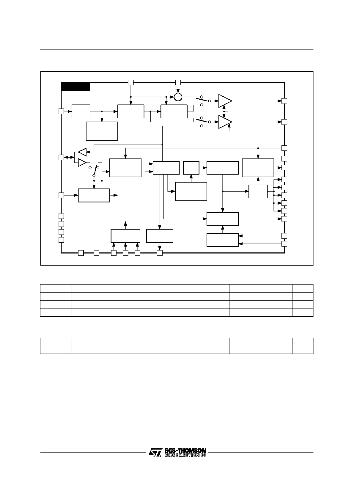
BLOCK DIAGRAM
STV5730A
VIDEO
2
CLAMP
7
19
5
6
21
20
LINE LOCKED
CS YNC
BAR
AV
DV
AGND
DGND
IN
DD
DD
COMPOSITE
SYNC
EXTRACTION
PLL
YIN CIN
28 25
SYNC
INSERTION
VERTICAL
SYNC
SEPARATION
PLXCLK
CONTROL
SERIALBUS
INTERFACE
11 1312 1043
INSERTION
H AND V
SCANNING
VIDEO
DETECTOR
MUTECSNCLKDATARESFTR
TEXT
GENERATOR
ASCII
RAM
RAM
ADDRESS
GAIN
DISABLE
CHARACTER
ROM
LUMA&SYNC
GENERATION
BIAS LEVEL
GENERATION
PAL/NTSC
ENCODER &
SATURATION
COLOR
LOGIC
STV5730A
VIDEO
27
OUT1
VIDEO
26
OUT2
XTAL
8
IN
XTAL
9
OUT
COUT
24
14
R
15
G
B
16
FB
17
CO
18
1
YOUT
LECHAR
22
LESCREEN
23
5730A-02.EPS
ABSOLUTEMAXIMUMRATINGS
Symbol Parameter Value Unit
DV
AV
DD
DD
T
Digital Supply Voltage 7 V
Analog Supply Voltage 7 V
Junction Temperature 150
j
THERMALDATA
Symbol Parameter Value Unit
R
th (j-a)
Junction-ambient Thermal Resistance Typ. 70
o
C/W
o
C
3/20
5730A-02.TBL
5730A-03.TBL

STV5730A
ELECTRICAL CHARACTERISTICS (TA=0oCto 70oC, AVDD=DVDD= 5V,unless otherwisespecified)
Symbol Parameter Min. Typ. Max. Unit
DV
DD
DI
DD
AV
DD
AI
DD
AV
-DVDDAnalog to Digital Supply Voltage Difference -200 0 200 mV
DD
DV
OH
DV
DV
DV
DI
IH
DI
IL
BW Bandwidth at pins : VIDEO IN, VIDEO OUT1,
VIDEO IN (Pin 2)
V
SYNCIN
V
CL
C
IN
VIDEO OUT1(Pin 27)
V
OUT1
C
L1
R
L1
Z
OUT1
VIDEO OUT2(Pin 26)
V
OUT2
C
L2
R
L2
Z
OUT2
GAIN (Pins 26- 27)
CIN (Pin 25)
C
CIN
R
CIN
YIN (Pin 28)
C
YIN
YOUT (Pin 1)
V
YOUT
C
LYOUT
R
LYOUT
COUT (Pin 24)
V
COUT
C
LCOUT
R
LCOUT
Digital Supply Voltage DVDD- DGND 4.75 5.0 5.25 V
Digital Supply Current 10 mA
Analog Supply Voltage 4.75 5.0 5.25 V
Analog Supply Current 25 mA
Digital Output Voltage High Level (I
Digital Output Voltage Low Level (I
OL
Digital Input Voltage High Level 0.75 x
IH
Digital Input Voltage Low Level 0.15 x
IL
= -1mA) DVDD-0.5 V
LOAD
= +1mA) DGND + 0.5 V
LOAD
- DGND)
(DV
DD
(DV
DD
Digital Input Current High Level 1 µA
Digital Input Current Low Level -1 µA
8.0 MHz
VIDEO OUT2, CIN, YIN, YOUT, COUT
Sync Pulse Range 100 650 mV
Clamp Voltage 1.10 1.30 1.50 V
External Capacitor 2.2 µF
Output Dynamic Range 2.0 4.4 V
Black Level Voltage 2.20 2.45 2.70 V
Output Capacitor Load 20 pF
Output Resistor Load 10 kΩ
Output Impedance 250 Ω
Output Dynamic Range 2.0 4.4 V
Black Level Voltage 2.20 2.45 2.70 V
Output Capacitor Load 20 pF
Output Resistor Load 10 kΩ
Output Impedance 250 Ω
Gain Dispersion 0dB
6dB
-1
5
0
6
Input Capacitance 0.5 pF
Input Resistance 50 kΩ
Input Capacitance 0.5 pF
Output Dynamic Range 0.5 3.5 V
Output Capacitor Load 15 pF
Output Resistor Load 10 kΩ
Output Dynamic Range 0.5 3.5 V
Output Capacitor Load 15 pF
Output Resistor Load 10 kΩ
- DGND)
+1
7
V
V
dB
dB
5730A-04.TBL
4/20

STV5730A
ELECTRICAL CHARACTERISTICS
=0oCto70oC, AVDD=DVDD=5V, unless otherwisespecified) (continued)
(T
A
Symbol Parameter Min. Typ. Max. Unit
LESCREEN (Pin 23)
V
LESCR
LECHAR (Pin 22)
V
LECH
INTERNAL SIGNAL LEVELS (Pins 1- 24)
V
SYNC
V
BLACK
V
SCREEN
V
CHAR
∆V1 Difference Level between Black and Sync Level 250 300 350 mV
∆V2 Difference Level between Screen and Black Level 100 150 200 mV
∆V3 Difference Level between Char. and Screen Level 450 515 580 mV
V
BURSTPP
V
CH1PP
V
CH2PP
BUS (Pins 11- 12 - 13)
f
CLK
t
CWL
t
CWH
t
CSWL
t
CSWH
t
DCLH
t
CLD
t
CLCSL
t
CSLCLL
t
CLHCSH
t
CSHCL
* maxHZ is the maximum horizontal zoom factor that is used
InputLevel 1.0 3.0 V
InputLevel 1.0 3.0 V
Internal Sync Level 0.95 V
Internal Black Level 1.1 1.25 1.4 V
Internal LESCREEN 1.4 V
Internal LECHAR 1.9 V
Burst Amplitude 320 mV
Chroma Amplitude for blue or yellow colors
for red, magenta, green or cyan colors
420
580
CLK Frequency Range 0 2 MHz
CLK Width Low 200 ns
CLK Width High 200 ns
CSN Width Low maxHZ* x 4 µs
CSN Width High maxHZ* x 4 µs
DATA Valid to CLK High 100 ns
CLK High to DATA Unvalid 100 ns
CLK Valid to CSN Low 100 ns
CSN Low to CLK Low 100 ns
CLK High to CSN High 100 ns
CSN High to CLK Unvalid 100 ns
mV
mV
PP
PP
PP
5730A-05.TBL
Figure1
DATA
CLK
t
CLCSL
CSN
t
DCLH
t
CSLCLL
t
t
CLD
t
CSHCL
t
CWL
t
CSWL
t
CWH
t
CLHCSH
t
CSWH
CLCSL
5730A-03.EPS
5/20

STV5730A
TYPICAL PAL/NTSC/SECAM APPLICATION
CVBS OUT
Ω
68
Ω
180
+5V
(see Note 1)
CHROMA BP FILTER
EXTERNAL
RGB
TEXT
INSERTION
Ω
68
(SCART)
+5V
Ω
68
Ω
180
+5V
+5V
+5V
Ω
180
68Ω
(see Note 3)
R1
+5V
Ω
Ω
180
68
CHROMA TRAP
20
9
220nF
+5V
17
18
19
0
A
10
11
12
39pF
Ω
180
15
16
13
14
39pF
TRANSLUCENT MODE
21
22
23
24
25
26
27
28
6
573
7
220nF
8
STV
LUMAFILTER (see Note 1)
F
µ
2.2
1
2
3
4
5
Ω
4.3k
H
µ
10
CVBS IN
(see note 4)
220pF
Notes : 1. Optional filter.For low cost applications, short circuit.
2. The 4fsc (17.734MHz PAL,14.318MHz NTSC) crystal may be ommited if this signal is already available in a system.
3. External bias level can be set by resistor ratio as required. The level atpins LECHAR and LESCREENmust not exceed 3.0 Vdc.
4. Output impedance of the driving stage should be less than 300Ω.
22kΩ
22nF
+5V
CSYNC
(INor OUT)
Ext. 4 fsc
XTAL
x 4fsc
OSC IN
(see Note 2)
TO MICRO
6/20
Digital Ground
Analog Ground
5730A-04.EPS
 Loading...