

SGS Thomson Microelectronics STV2001 Datasheet
STV2001
I2C SINGLE FREQUENCY DEFLECTION PROCESSOR
AND 120 MHz RGB PREAMPLIFIER
TARGET SPECIFICATION
FEATURES
Horizontal deflection
■ Single Frequ enc y, Se lf Adapt ive Os c illa tor.
■ TTL compatible positive going sync.
■ Chip does not accept sync on RGB or any video
signal.
2
■ I
C controlled: H-position, pin cushion,
keystone, parallelogram, side pin balance.
2
■ I
C controlled EW corner : top and bottom
corrections.
2
■ I
C controlled corner: top and bottom phase
corrections.
■ EW output
2
■ I
C controlled H-amplitude
■ DC controlled H-width breath ing comp ensation
■ Xray shut-down on ABL, H output latch, reset by
■ Soft start on H-duty.
Ver tical deflection
■ Vertical ramp generator.
■ Wide range AGC loop.
■ TTL compatible positive going sync, no extra
■ I
■ I
■ DC controlled height breathing compensation
■ Vertical dynamic focus output with fixed
Video preamplifier
■ 3-Channel 120MHz bandwidth video amplifier.
■ 3.5ns typical rise and fall time at 2.5V
■ I
■ I
■ Activation of ABL results in contrast gain
2
with I
C controlled gain (0.5x to 2x).
power OFF/ON.
pulses.
2
C controlled vertical position.
2
C controlled S linearity correction.
2
with I
C controlled gain (0.5X TO 2X).
amplitude (1Vpp).
.
2
C controlled individual RGB contrast
PP
(8bit)>8db
2
C controlled overall brightness.
decrease.
■ Gain window (1.5X) controlled by input pulse
2
and I
C. Pulse height controls the gain variation
from 1x to 1.5x.
■ 0.514V typical video input signal for normal
display.
2
■ I
C controlled contrast (7bits) update during
vertical retrace time.
2
C main features
I
2
■ I
C interface (slave) 100kHz max.
2
■ All I
C controlled DAC are 7 bits, except R GB
gain.
■ Power on reset on 5 V (V
DD
).
Supply voltage & power
■ 5 V/10.5 V dual supply.
■ Max power consumption: 1.2W
DESCRIPTION
The STV2001 is an I2C-controlled monolithic
integrated circuit assembled in a TQF P44 plastic
package. It combines both a deflection block
(horizontal and vertical, single frequency with very
powerful geometry correction) and a 120MHz
RGB pre-amplifier.
TQFP44/SLUG DOWN
ORDER CODE :
Version 1.2
May 2000 1/46
This is preliminary information on a new product now in development. Details are subject to change without notice.
1

TABLE OF CONTENTS
1 - PIN CONNECTIONS . . . . . . . . . . . . . . . . . . . . . . . . . . . . . . . . . . . . . . . . . . . . . . . . . . . . . . . . . . 4
2 - PIN DESCRIPTION . . . . . . . . . . . . . . . . . . . . . . . . . . . . . . . . . . . . . . . . . . . . . . . . . . . . . . . . . . . 5
3 - BLOCK DIAGRAM . . . . . . . . . . . . . . . . . . . . . . . . . . . . . . . . . . . . . . . . . . . . . . . . . . . . . . . . . . . 6
4 - ABSOLUTE MAXIMUM RATINGS . . . . . . . . . . . . . . . . . . . . . . . . . . . . . . . . . . . . . . . . . . . . . . . 7
5 - THERMAL DATA . . . . . . . . . . . . . . . . . . . . . . . . . . . . . . . . . . . . . . . . . . . . . . . . . . . . . . . . . . . . 7
6 - SYNC INPUT . . . . . . . . . . . . . . . . . . . . . . . . . . . . . . . . . . . . . . . . . . . . . . . . . . . . . . . . . . . . . . . . 7
7 - I2C READ/WRITE . . . . . . . . . . . . . . . . . . . . . . . . . . . . . . . . . . . . . . . . . . . . . . . . . . . . . . . . . . . . 8
8 - HORIZONTAL SECTION . . . . . . . . . . . . . . . . . . . . . . . . . . . . . . . . . . . . . . . . . . . . . . . . . . . . . . 8
9 - VERTICAL SECTION . . . . . . . . . . . . . . . . . . . . . . . . . . . . . . . . . . . . . . . . . . . . . . . . . . . . . . . . 10
10 - VIDEO PRE-AMP SECTION . . . . . . . . . . . . . . . . . . . . . . . . . . . . . . . . . . . . . . . . . . . . . . . . . . 13
11 - LOGIC SECTION . . . . . . . . . . . . . . . . . . . . . . . . . . . . . . . . . . . . . . . . . . . . . . . . . . . . . . . . . . 15
12 - I2C BUS ADDRESS TABLE . . . . . . . . . . . . . . . . . . . . . . . . . . . . . . . . . . . . . . . . . . . . . . . . . . 16
13 - TYPICAL OUTPUT WAVEFORMS . . . . . . . . . . . . . . . . . . . . . . . . . . . . . . . . . . . . . . . . . . . . . 19
14 - OPERATING DESCRIPTION . . . . . . . . . . . . . . . . . . . . . . . . . . . . . . . . . . . . . . . . . . . . . . . . . 24
14.1 -GENERAL CONSIDERATIONS . . . . . . . . . . . . . . . . . . . . . . . . . . . . . . . . . . . . . . . . . . . . 24
14.1.1 -Power Supply . . . . . . . . . . . . . . . . . . . . . . . . . . . . . . . . . . . . . . . . . . . . . . . . . . . . 24
14.1.2 -I
14.1.3 -Write Mode . . . . . . . . . . . . . . . . . . . . . . . . . . . . . . . . . . . . . . . . . . . . . . . . . . . . . . 24
14.1.4 -Read Mode . . . . . . . . . . . . . . . . . . . . . . . . . . . . . . . . . . . . . . . . . . . . . . . . . . . . . . 24
14.1.5 -Sync Processor . . . . . . . . . . . . . . . . . . . . . . . . . . . . . . . . . . . . . . . . . . . . . . . . . . . 24
14.1.6 -IC Status . . . . . . . . . . . . . . . . . . . . . . . . . . . . . . . . . . . . . . . . . . . . . . . . . . . . . . . . 24
14.1.7 -Sync Inputs . . . . . . . . . . . . . . . . . . . . . . . . . . . . . . . . . . . . . . . . . . . . . . . . . . . . . . 24
14.1.8 -Sync Processor Output . . . . . . . . . . . . . . . . . . . . . . . . . . . . . . . . . . . . . . . . . . . . . 25
14.2 -HORIZONTAL PART . . . . . . . . . . . . . . . . . . . . . . . . . . . . . . . . . . . . . . . . . . . . . . . . . . . . 25
14.2.1 -Internal Input Conditions . . . . . . . . . . . . . . . . . . . . . . . . . . . . . . . . . . . . . . . . . . . . 25
14.2.2 -PLL1 . . . . . . . . . . . . . . . . . . . . . . . . . . . . . . . . . . . . . . . . . . . . . . . . . . . . . . . . . . . 25
14.2.3 -PLL2 . . . . . . . . . . . . . . . . . . . . . . . . . . . . . . . . . . . . . . . . . . . . . . . . . . . . . . . . . . . 27
14.2.4 -Output Section . . . . . . . . . . . . . . . . . . . . . . . . . . . . . . . . . . . . . . . . . . . . . . . . . . . 27
14.2.5 -X-RAY Protection . . . . . . . . . . . . . . . . . . . . . . . . . . . . . . . . . . . . . . . . . . . . . . . . . 28
14.3 -VERTICAL PART . . . . . . . . . . . . . . . . . . . . . . . . . . . . . . . . . . . . . . . . . . . . . . . . . . . . . . . 28
14.3.1 -Function . . . . . . . . . . . . . . . . . . . . . . . . . . . . . . . . . . . . . . . . . . . . . . . . . . . . . . . . 28
14.3.2 -I2C Control Adjustments . . . . . . . . . . . . . . . . . . . . . . . . . . . . . . . . . . . . . . . . . . . . 28
14.3.3 -Basic Equations . . . . . . . . . . . . . . . . . . . . . . . . . . . . . . . . . . . . . . . . . . . . . . . . . . 29
14.3.4 -Geometric Corrections . . . . . . . . . . . . . . . . . . . . . . . . . . . . . . . . . . . . . . . . . . . . . 29
14.3.5 -E/W . . . . . . . . . . . . . . . . . . . . . . . . . . . . . . . . . . . . . . . . . . . . . . . . . . . . . . . . . . . . 32
14.3.6 -Dynamic Horizontal Phase Control . . . . . . . . . . . . . . . . . . . . . . . . . . . . . . . . . . . . 32
14.3.7 -Vertical Dynamic Focus . . . . . . . . . . . . . . . . . . . . . . . . . . . . . . . . . . . . . . . . . . . . 32
14.3.8 -Corner Correction . . . . . . . . . . . . . . . . . . . . . . . . . . . . . . . . . . . . . . . . . . . . . . . . . 32
14.3.9 -Horizontal Breathing . . . . . . . . . . . . . . . . . . . . . . . . . . . . . . . . . . . . . . . . . . . . . . . 32
14.3.10 -Vertical Breathing . . . . . . . . . . . . . . . . . . . . . . . . . . . . . . . . . . . . . . . . . . . . . . . . 32
14.4 -GENERAL CONSIDERATIONS . . . . . . . . . . . . . . . . . . . . . . . . . . . . . . . . . . . . . . . . . . . . 32
14.4.1 -Input Stage . . . . . . . . . . . . . . . . . . . . . . . . . . . . . . . . . . . . . . . . . . . . . . . . . . . . . . 3 2
14.4.2 -Contrast Adjustment (7 bits) . . . . . . . . . . . . . . . . . . . . . . . . . . . . . . . . . . . . . . . . . 33
14.4.3 -ABL Control . . . . . . . . . . . . . . . . . . . . . . . . . . . . . . . . . . . . . . . . . . . . . . . . . . . . . . 33
14.4.4 -Brightness Adjustment (6 bits) . . . . . . . . . . . . . . . . . . . . . . . . . . . . . . . . . . . . . . . 33
14.4.5 -Drive Adjustment (3 x 8 bits) . . . . . . . . . . . . . . . . . . . . . . . . . . . . . . . . . . . . . . . . . 33
14.4.6 -Output Stage . . . . . . . . . . . . . . . . . . . . . . . . . . . . . . . . . . . . . . . . . . . . . . . . . . . . . 33
14.4.7 -Bright Window . . . . . . . . . . . . . . . . . . . . . . . . . . . . . . . . . . . . . . . . . . . . . . . . . . . . 35
2
C Control . . . . . . . . . . . . . . . . . . . . . . . . . . . . . . . . . . . . . . . . . . . . . . . . . . . . . . 24
3
2/3
2

14.4.8 -Blanking Generator . . . . . . . . . . . . . . . . . . . . . . . . . . . . . . . . . . . . . . . . . . . . . . . . 35
14.5 -GENERAL CONSIDERATIONS . . . . . . . . . . . . . . . . . . . . . . . . . . . . . . . . . . . . . . . . . . . . 36
14.5.1 -POR (Power On Reset) - Subad. 11-D8 . . . . . . . . . . . . . . . . . . . . . . . . . . . . . . . . 36
14.5.2 -Supply Voltage Threshold. . . . . . . . . . . . . . . . . . . . . . . . . . . . . . . . . . . . . . . . . . . 36
14.5.3 -Video Off (I2C control) - Subad. 00-D8 . . . . . . . . . . . . . . . . . . . . . . . . . . . . . . . . . 36
14.5.4 -Vertical Output Off . . . . . . . . . . . . . . . . . . . . . . . . . . . . . . . . . . . . . . . . . . . . . . . . 36
14.5.5 -X-Ray, Set Operation - Subad. 09-D8 . . . . . . . . . . . . . . . . . . . . . . . . . . . . . . . . . 36
15 - INTERNAL SCHEMATICS . . . . . . . . . . . . . . . . . . . . . . . . . . . . . . . . . . . . . . . . . . . . . . . . . . . 37
16 - PACKAGE MECHANICAL DATA . . . . . . . . . . . . . . . . . . . . . . . . . . . . . . . . . . . . . . . . . . . . . . 45
3/3
STV2001
1 - PIN CONNECTIONS
Hin
Vin
Vref
VAGCCAP
VGND
VCAP
Vout
VRB
VAVcc
OUT1
AGND
FC1
FILTER
44 43 42 41 40 39 38 37 36 35 34
1
2
3
4
5
6
7
8
9
10
11
12 13 14 15 16 17 18 19 20 21 22
OUT3
OUT2
PGND
Co
Ro
PVCC
PLL1F
VBCAP
PLL2C
HGND
IN1
IN2
ABLin
VBDC
GAINWIN
Hfly
Href
Hout
33
32
31
30
29
28
27
26
25
24
23
HDGND
LGND
SAVcc
SCL
SDA
V
(5V)
DD
EWout
FCAP
HBRTHin
VBRTHin
VFOCUS
IN3
VFLYin
4/46
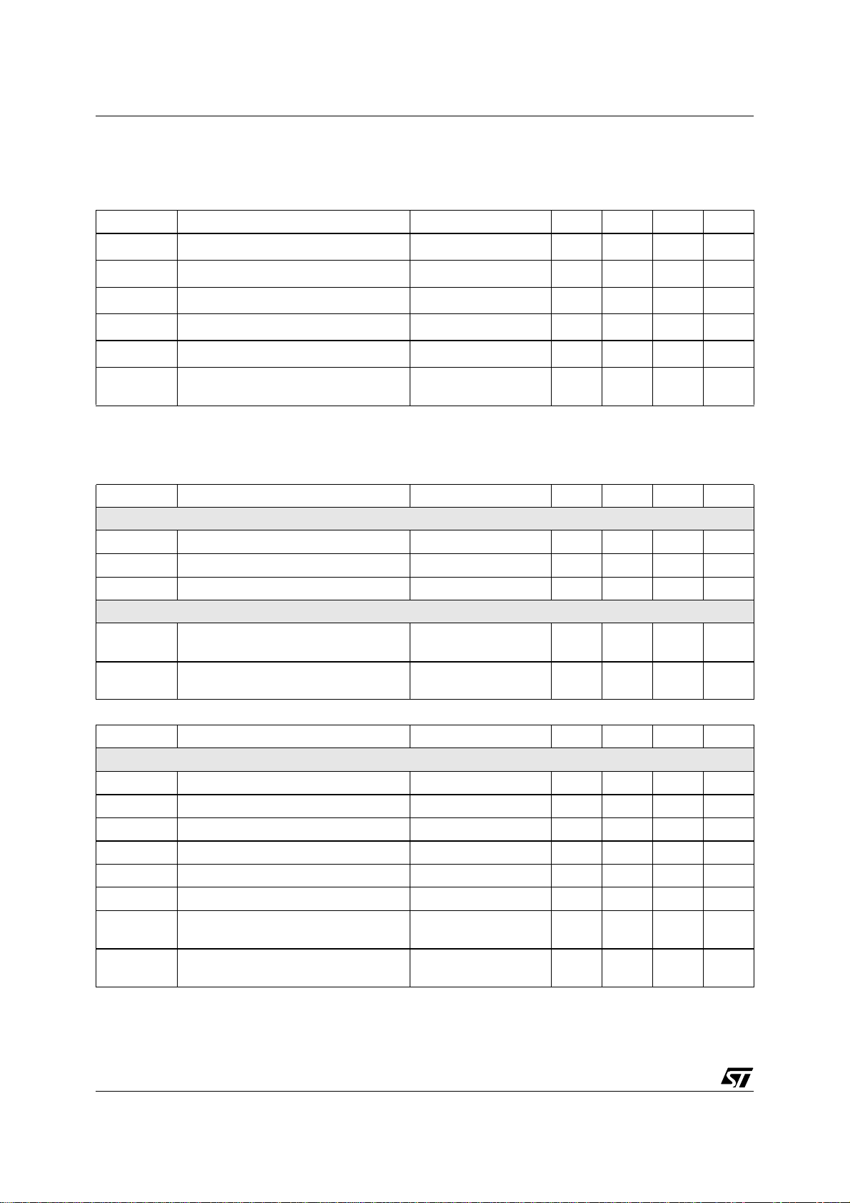
3
2 - PIN DESCRIPTION
Pin Name Function
1 Hin Horizontal Sync Input
2 Vin Vertical Sync Input
3 Vref Vertical Section Reference Voltage
4 VAGCCAP Vertical AGC Loop Capacitor
5 VGND Vertical Section Ground
6 VCAP Vertical Sawtooth Generator Capacitor
7 Vout Vertical Output
8 VRB Vertical Ramp Filter
9 VAVcc Video Section Analog Supply (10.5V typ)
10 OUT1 Video Output 1
11 AGND Video Analog Ground
12 OUT2 Video Output 2
13 PGND Video Section Power Ground
14 OUT3 Video Output 3
15 PVcc Video Section Power Supply (10.5V typ)
16 GAINWIN Gain Window Input
17 IN1 Video Input 1
18 VBDC Vertical Blanking Output with DC Level adjusted by DAC
19 IN2 Video Input 2
20 ABLin Video Automatic Beam Current Compensation Input
21 IN3 Video Input 3
22 VFLYin Vertical Fly Back Pulse Input
23 VFOCUS Vertical Dynamic Focus Output
24 VBRTHin Vertical Breathing DC Input
25 HBRTHin Horizontal Breathing Compensation DC Input
26 FCAP Filter Capacitor
27 EWout EW Output
28 V
29 SDA I
30 SCL I
31 SAVcc Scanning Section Analog Supply (10.5Vtyp)
32 LGND Bus and Scanning Power Ground
33 HDGND H Driver Output Ground
34 Hout Horizontal Driver Output, open collector
35 Href Horizontal Section Reference Voltage
36 Hfly Horizontal Flyback Input, Positive
37 HGND Horizontal Section Ground
38 PLL2C PLL2 Loop Filter
39 VBCAP PLL2 Top Comparator Filter
40 PLL1F PLL1 Loop Filter
41 Ro Horizontal Oscillator Resistor
42 Co Horizontal Oscillator Capacitor
43 FC1 PLL1 Filter Capacitor
44 FILTER Horizontal Filter Capacitor (HPOS)
DD
Bus, Scanning Logic and Video Logic Supply (5V typ)
2
C Data Input
2
C Clock Input
STV2001
5/46

6/46
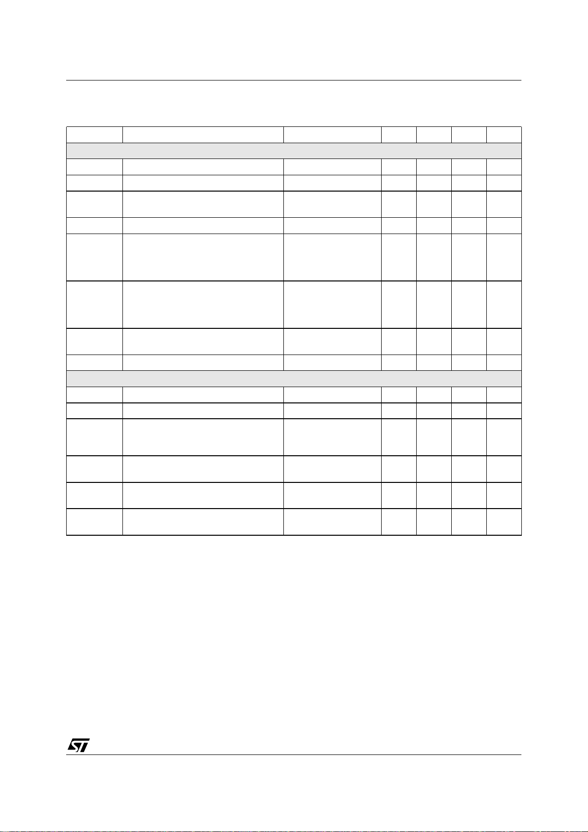
3 - BLOCK DIAGRAM
STV2001
SAV
CC
Href
Vref
Hin
Vin
HGND
VGND
VCAP
VAGCCAP
VRB
Vout
VFOCUS
SDA
SCL
VDD
LGND
IN1
IN2
GAINWIN
IN3
31
35
3
1
2
37
5
6
4
8
7
23
29
30
28
32
17
19
16
21
Href
Scorr
Hsync
Gain
WIndow
PLL1F FILTER FC1 Ro Co HFly PLL2C Hout
40
Vref
Vpos
VOSC
RAMP
Generator
VDF
2
C BUS
I
DECODER
Clamp
44 43 41 42 36 38
Phase
Freq
Comp
Vamp
VCO
Corner
Phase
Geometry
Tracking
EW
Corner
LATCHES & DACs
BrightnessContrast
Phase
Comp
2
X
KeyBal
X
SPB
Drive
VBCAP
39
Phase
Shifter
X
+
HFly
Hsync
Vsync
EWPCC
2
KEYST
34 33
HOUT
Buffer
EW OUTPUT
H Breathing
+
Blanking
BPCP
Output
Stage
HDGND
Safety
VFBack
EHTcomp
AMP
ABL
EWout
27
FCAP
26
22
VFLYin
18
VBDC
25
HBRTHin
VBRTHin
24
VAV
9
OUT 1
10
AGND
11
PV
15
12
OUT 2
ABLin
20
PGND
13
OUT 3
14
CC
CC
STV2001
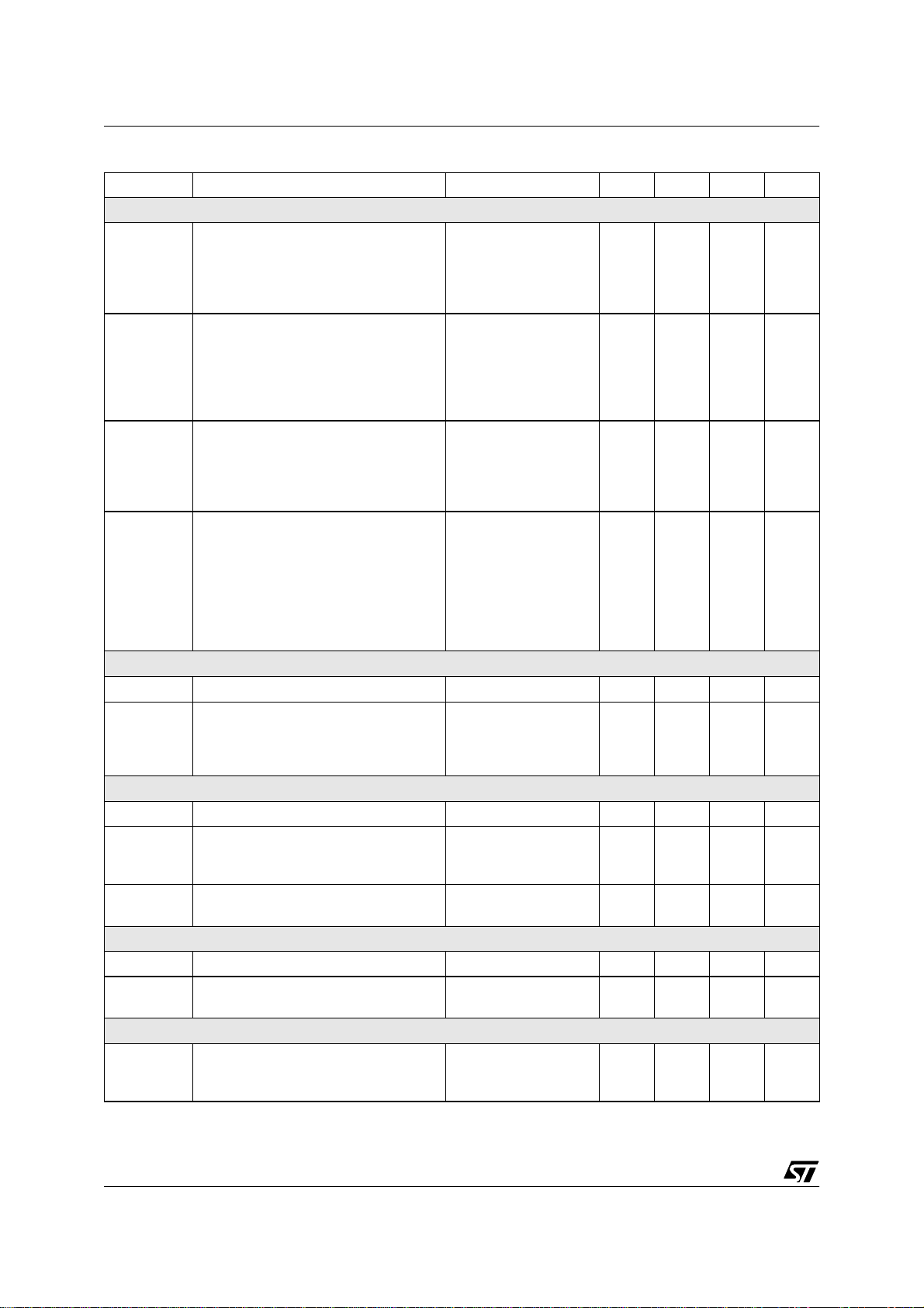
4 - ABSOLUTE MAXIMUM RAT INGS
Symbol Parameter Value Unit
SAVcc Scanning Section Analog Supply Voltage 13.5 V
VAVcc Video Section Analog Supply Voltage 13.5 V
PVcc Supply Voltage for Video Pre-Amp Section 13.5 V
Vdd Logic Section Supply Voltage 5.5 V
V
ESD
Tstg Storage Temperature -40 to 150
Tj Junction Temperature 150
Toper Operating Temperature (Device ambient) 0 to 70
ESD susceptibility HBM model 100pF & 1.5kΩ
EIAJ Norm 200pF & 0Ω
2
300
5 - THERMAL DAT A
STV2001
kV
V
o
C
o
C
o
C
Symbol Parameter Value Unit
R
TH(j-a)
Junction to Ambient Thermal Resistance (MAX) 46
6 - SYNC INPUT
Operating Conditions (V
Symbol Parameter Test Conditions Min Typ Max Unit
HSVR Voltage on Hin 0 5 V
MinD Min Hin pulse duration 0.7 us
Mduty Max Hin Duty Cycle 25 %
VSVR Voltage on Vin 0 5 V
VSW Min Vin pulse duration 5 us
VSD Max Vin Duty Cycle 15 %
Electrical Characteristics (VDD = 5V, T
V
INTH
RIN Horizontal & Vertical Pull-Up Resistor 200 kΩ
Horizontal & Vertical Input Logic Level Low Level
= 5V, T
DD
amb
= 25°C)
= 25°C)
amb
0.8 V
High Level 2.2
o
C/W
V
7/46
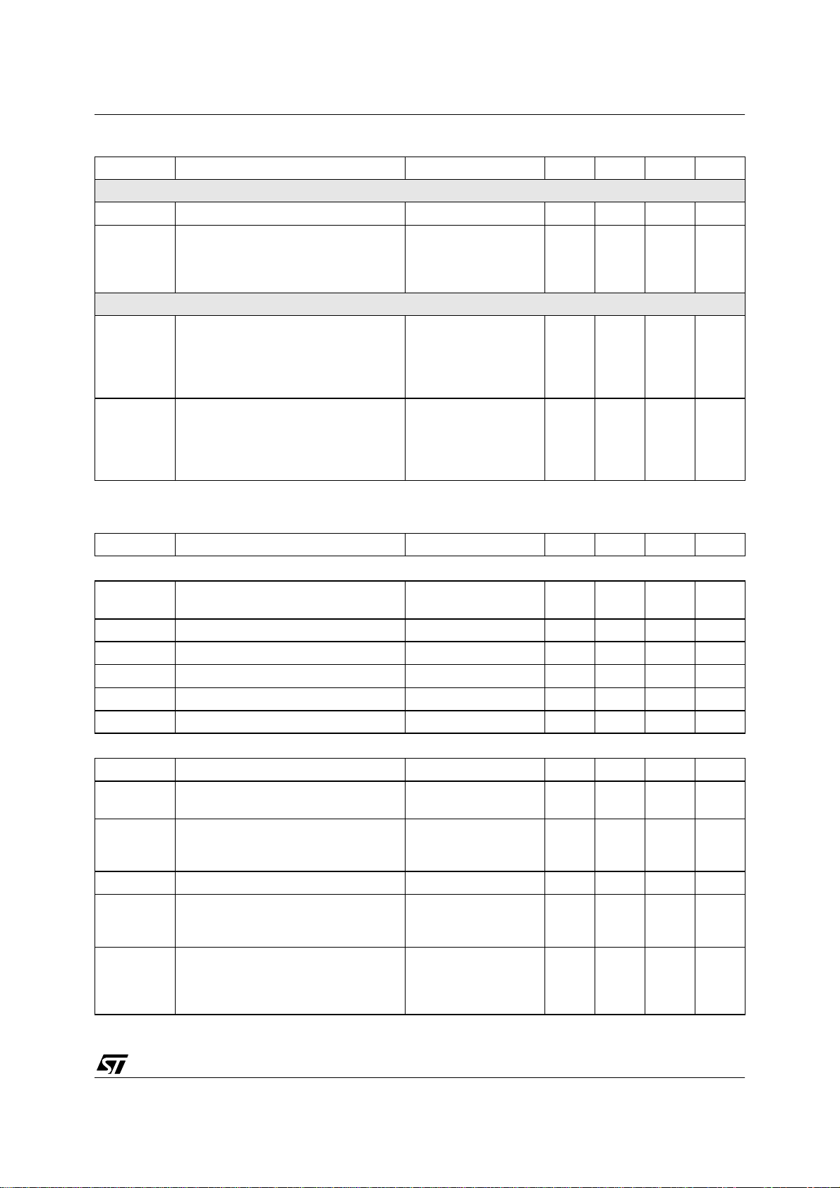
STV2001
7 - I2C READ /WRITE
Electrical Characteristics (VDD = 5V, T
amb
= 25°C)
Symbol Parameter Test Conditions Min Typ Max Unit
F
T
T
HIGH
V
V
V
SCL
LOW
INL
INH
ACK
Maximum Clock Frequency 100 kHz
Low Period of the SCL Clock 1.3 us
High Period of SCL Clock 0.6 us
SDA & SCL Input Low Level Voltage 1.5 V
SDA & SCL Input High Level Voltage 3 V
Acknowledge Output Voltage on SDA
input with 3mA
0.4 V
8 - HORIZONTAL SECTION
Operating Conditions
Symbol Parameter Test Conditions Min Typ Max Unit
VCO
Ro(min) Minimum Oscillator Resistor 6 kΩ
Co(min) Minimum Oscillator Capacitor 390 pF
Fmax Maximum Oscillator Frequency 150 kHz
OUTPUT SECTION
I
HFB
I
HOUT
Horizontal FlyBack Input Maximum
Current
Horizontal Drive Output Maximum Sink
Current
5mA
15 mA
Electrical Characteristics (VDD = 5V, T
amb
= 25°C)
Symbol Parameter Test Conditions Min Typ Max Unit
SUPPLY AND REFERENCE VOLTAGES
Vcc Supply Voltage 9.5 10.5 11.5 V
Vdd Supply Voltage 4.5 5 5.5 V
Icc Supply Current 30 mA
Idd Supply Current 5 mA
V
HREF
Horizontal Reference Voltag e I=-2mA 7.4 8 8.6 V
VVREF Vertical Reference Voltage I=-2mA 7.4 8 8.6 V
I
HREF
I
VREF
Horizontal Reference Maxim um Source
Current
Vertical Reference Maximum Source
Current
5mA
5mA
8/46
STV2001
Operating Conditions
Symbol Parameter Test Conditions Min Typ Max Unit
1st PLL SECTION
V
clamp
V
VCO
A
VCO
H
PHASE
VPMIN
VPTYP
VPMAX
I
PLL1-UL
I
PLL1-L1
I
PLL1-L2
f
O
dfo/dT Free Running Frequency Thermal Drift -150 ppm/
2nd PLL SECTION & HORIZONTAL OUTPUT SECTION
V
THFB
Jitter
H
DC
Vphi2 Internal Clamp Level on PLL2 Filter
VSCinh
Vsat
VCO clamp Voltage range V
VCO clamp Voltage, at POR V
VCO Gain
=8V 3.0 3.8 V
HREF
=8V 3.8 V
HREF
Ro=4868Ω, Co=820pF,
dF/dV=1/11RoCo
23 kHz/V
Horizontal Phase Adjustment Range % of Horizontal Period +/-10 %
Horizontal Phase Setting
Minimum
Typical
Maximum
PLL1 Charge Pump Current
Unlocked
Locked
Locked
Free Running Frequency, no input
at POR, lower clamp voltage at max.
SubAdd 07
X1111111
X1000000
X0000000
2.8
3.4
4.0
Sub-Address 11
+/-40
x1xx xxxx
x0xx xxxx
+/-1
±300
Ro=4868Ω, Co=820pF 86 kHz
Flyback Input Threshold Voltage 0.65 0.75 V
Horizontal Jitter At 80KHz 70 ppm
H
Horizontal Drive Output Duty Cycle
(Ratio of Power Transistor OFF time to
55 %
Period)
Threshold Voltage to Stop H-Out, V-Out,
Reset ABL when Vcc<VSCinh
Horizontal Drive Output Saturatio n
HD
Voltage
Low Level
High Level
Iout=15mA 0.4 V
1.6
4.0
6.9 V
V
V
V
µA
mA
µA
V
V
o
C
9/46
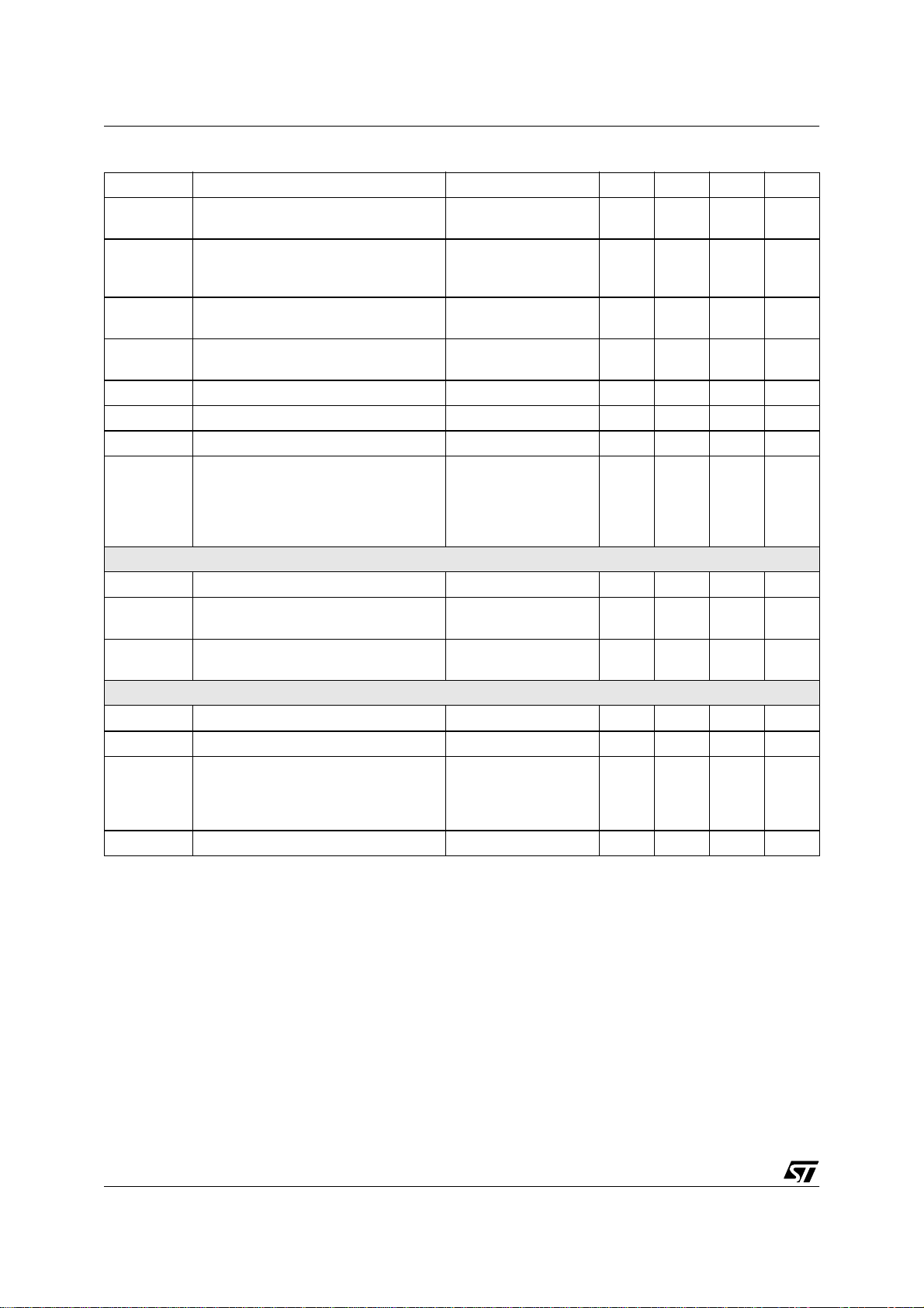
STV2001
9 - VERTICAL SECTION
Symbol Parameter Test Conditions Min Typ Max Unit
Electrical Characteristics (VDD = 5V, T
amb
VERTICAL RAMP SECTION
V
RBOT
V
RTOP
V
RTOPF
T
VDIS
F
FRV
Voltage at Ramp Bottom Point V
Voltage at Ramp Top Point with Sync V
Voltage at Ramp Top Point without Sync V
Vertical Sawtooth Discharge Time C
Vertical Free Running Frequency
(S correction inhibited)
ASFR Auto- Sync Frequ ency Range C
RAFD
R
LIN
V
POS
Ramp Amplitude Drift Versus Frequency
at Maximum Vertical Amplitude
Ramp Linearity at Vcap pin
with S Correction inhibited
Vertical Position Adjustment Voltage
with V
mean value
OUT
VOR Vertical Output Peak to Peak Voltage
I
VOUT
V
VRB
Vertical Output Maximum Current +/-5 mA
Vertical Ramp Filter Voltage 2 V
Max Vertical S-Correction Amplitude
dVS
S-Correction inhibited, DV/Vpp at TV/4
S-correction Maximum,
DV/Vpp at 3TV/4
= 25°C)
=8V 2 V
VREF
=8V 5 V
VREF
-
V
=8V
VREF
=150nF 70 µs
OSC
C
=150nF 100 Hz
OSC
=150nF 50 16 5 Hz
OSC
C
=150nF 50Hz -
OSC
165Hz
2.5V < VOSC < 4.5V 0.5 %
Sub-Add=09
X0000000
X1000000
X1111111 3.65
Sub-Add=08
10000000
11000000
11111111 3.5
Sub-Add 0A
0XXXXXXX
11111111
RTOP
0.1
200 ppm/Hz
3.2
3.5
3.8
2.25
3
3.75
-4
+4
V
3.3 V
V
V
2.5 V
V
V
%
%
10/46
STV2001
Symbol Parameter Test Conditions Min Typ Max Unit
EAST/WEST FUNCTION (available without feedback connection)
DC Output Voltage with:
EW
DC
TDEW
DC
EW
PARA
EW
track
KeyAdj
KeyTrack
EW Corner
Top
EW Corner
Bottom
-Typical VPOS and Keystone inhibited
-External driver connected as unity gain
buffer
DC Output Voltage Thermal Drift
(Non-test Parameter)
Parabola Amplitude with:
-Max VAMP
-Typ VPOS
-Keystone inhibited
Parabola Amplitude Function of VAMP
Control (tracking between VAMP & EW)
with:
-Typ VPOS=typ.
-Keystone=typ.
-EW Amplitude=typ.
Keystone Adjustment Capa bility with:
-VPOS=typ.
-EW= inhibited
-Vertical Amplitude= Max.
Intrinsic Keystone Function of VPOS
Control (tracking between VPOS and
EW) with :
-EW Amplitude= Max
-Vertical Amplitude=Max
A/B Ratio
B/A Ratio
Corner Adjustment capability with :
-VPS=typ,
-EW = inhibited
-VAMP = max
-HSize = Min
-HBreath>VREF
-Keystone = inhibited
Corner Adjustment capability with :
-VPS=Typ,
-EW = inhibited
-VAMP = Max
-HSize = Min
-HBreath>VREF
-Keystone = inhibited
Sub-add 0C
11111111
11000000
10000000
Sub-address 08
10000000
11000000
11111111
Sub-address 0B
10000000
11111111
Sub-address 09
X0000000
X1111111
Sub-address 04
1111 1111
1100 0000
1000 0000
Sub-address 15
1111 1111
1100 0000
1000 0000
2.0 V
100 ppm/
1.0
0.5
0
0.18
0.35
0.57
0.2
0.2
0.52
0.52
+1.25
0
-1.25
+1.25
0
-1.25
V
V
V
V
V
V
V
pp
V
pp
Vpp
Vpp
Vpp
Vpp
Vpp
Vpp
o
C
11/46
STV2001
Symbol Parameter Test Conditions Min Typ Max Unit
INTERNAL DYNAMIC HORIZONTAL PHASE CONTROL
Side Pin Balance Parabola Amplitude
with:
SBPpara
-VAMP=Max,
-VPOS=typ.
-Parallelogram inhibited
Side Pin Balance Parabola Amplitude
function of VAMP Control (tracking be-
SPBtrack
tween VAMP & SPB) with
-SPB=Max
-VPO=typ.
-Parallelogram= inhibi ted
Parallelogram Adjustment Capability
with:
ParAdj
-VAMP=Max
-POS =Typ
-SPB=Max
Intrinsic Parallelogram Function of
VPOS Control (tracking between VPOS
and DHPC) with
Partrack
-VAMP=Max
-SPB=Max
-Parallelogram= inhibi ted
A/B Ratio
B/A Ratio
VERTICAL BREATHING COMPENSATION
VBRrng Input DC Breathing Control Range 1 10.5 V
Vertical Size Compensation
VSC
Variation of V output vs full range of
VBRrng
VERTICAL DYNAMIC FOCUS OUTPUT
VDF
DC Output Level RL=10kΩ 4V
DC
VDF Parabola Amplitude with:
VDFamp
Vamp = typ
VPOS = typ.
V
FOCPOL
Parabola Polarity at Output =
Inverted “U”
VERTICAL FLYBACK INPUT
V
FLYTH
V
FLYINH
Vertical Flyback Threshold 1 V
Inhibition of Vertical Flyback input
(id pulse in action instead of VFlyback)
HORIZONTAL SIZE CONTROL
Hsize Hsize output DC voltage
sitting on top of EWDC=2.0V
Sub-add 0E
11111111
10000000
Sub-add 08
10000000
11000000
11111111
Sub-add 0F
11111111
10000000
Sub-add 09
X0000000
X1111111
Sub-address 14
XX00 0000
X100 0000
XX11 1111
sub-add 0D
X0000000
X1111111
+1.4
-1.4
0.5
0.9
1.4
+1.4
-1.4
0.52
0.52
-5
-20
1 Vpp
6.5 V
0
2.4
%T
%T
%T
%T
%T
%T
%T
%
%
%
H
H
H
H
H
H
H
V
V
12/46
STV2001
Symbol Parameter Test Conditions Min Typ Max Unit
HORIZONTAL BREATHING COMPENSATION
HBRrng Breathing input DC Control Range 1 10.5 V
Horizontal size compensation, EW DC
HSC
voltage variation under full range of
HBRrng
CORNER PHASE CORRECTION
Corner Phase Top Adjustment with:
Corner
Phase Top
Vamp = max
Vpos = Typ.
SPB = OFF
Parrallelogram = OFF
Corner Phase Bottom Adjustment with:
Corner
Phase
Bottom
Vamp = max
Vpos = Typ.
SPB = OFF
Parrallelogram = OFF
Sub-address 12
X000 0000
X100 0000
X111 1111
Sub-address 05
1000 0000
1111 1111
Sub-address 06
0000 0000
0111 1111
0.2
0.8
-2.8
+2.8
-2.8
+2.8
V
V
%
%
%
%
10 - VIDEO PRE-A MP SECTION
Symbol Parameter Test Conditions Min Typ Max Unit
DC Electrical Characteristics (VAV
VAV
cc
Video Section Analog Supply Voltage
PVcc Power Section Supply Voltage 9.5 10.5 11.5 V
IS Supply Current of VAVcc & PVcc 63 mA
V
V
V
IN
OUT
Black
Video Input Voltage Amplitude 0.7 1 Vpp
Typical Output Voltage Range 0.5 7 V
Output (Black level) 1.5 V
AC Electrical Characteristics (VAVCC = PV
Symbol Parameter Condition Min Typ Max Unit
AV Maximum Gain
CAR Contrast Attenuation Range
DAR Drive Attenuation Range 30 dB
GM Gain Match
BW Large Signal Bandwidth
CC
= PV
= 10.5V, Tamb = 25oC)
CC
9.5 10.5 11.5 V
= 10.5V, CL = 5pF, RL = 1KΩ, Tamb = 25oC)
CC
Max Contrast and Drive
2
I
C Gainwin = 1
V
= 0.7Vpp
IN
Contrast and Drive at
18 dB
30 dB
POR
V
= 0.7Vpp,
IN
V
= 4Vpp, Contrast
OUT
+-0.1 dB
and Drive= 0.87Max
V
=0.7Vpp,
IN
= 2.5Vpp, Contrast
V
OUT
and Drive = 0.87Max
120 MHz
At -3dB
13/46
STV2001
Symbol Parameter Test Conditions Min Typ Max Unit
DIS Video Output Distortion f=1MHz, VIN=1Vpp,
V
= 1Vpp
OUT
= 0.7Vpp,
V
, t
t
R
Video Output Rise and Fall Time
F
IN
V
=2.5Vpp,Contrast
OUT
and Drive=0.87Max
dVo Overshoot of output with respect to
actual output amplitude
=5pF 5 7 %
C
LOAD
BRT Brightness max DC level
Brightness min DC level
R
L
Equivalent Load on Video Output Tj<Tj
MAX
Tsample Hold time 100 ms
Thold Sample time 1 µs
V
= 0.7Vpp,
CT Crosstalk Between Video Channels
IN
V
= 2.5Vpp,
OUT
Contrast and
44 dB
Drive=0.7Max
f=1MHz
ABL COMPENSATION
R
G
TH
ABL
ABL
ABL
ABL Input resistor 10 kΩ
ABL minimum Attenuation
ABL maximum Attenuation
ABL latch function activation threshold
(High beam current detection)
V
=5.3V
ABL
V
=2.8V
ABL
01V
GAIN WINDOW
V
INL
V
INH
Input Low Level Voltage 0.7 V
Input High Level Voltage 1.5 V
Contrast Gain Increase during High
Gain
Input
VIN = 1.5V
VIN = 5.0V
T
D
Total Delay Time 100 ns
0.3 %
3.5 4 ns
2.5
0
1kΩ
0
12
1
1.5
V
V
dB
dB
V/V
V/V
14/46
 Loading...