

SGS Thomson Microelectronics STV160NF03L Datasheet
STV160NF03L
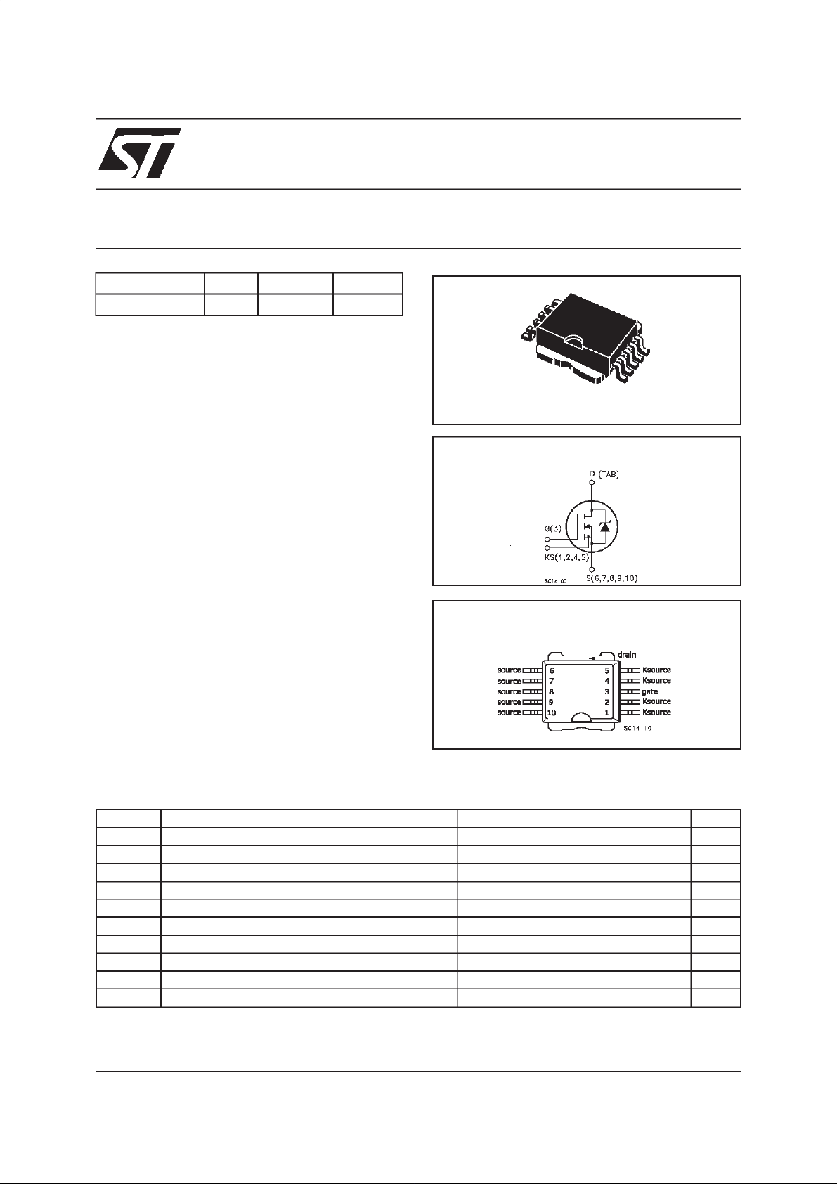
N - CHANNEL 30V - 0.0019Ω - 160A PowerSO-10
STripFET MOSFET
TYPE V
DSS
R
DS(on)
I
D
ST V160NF03L 30 V < 0.0028 Ω 160 A
■ TYPICALR
■ ULTRA LOW ON-RESISTANCE
■ ULTRA FAST SWITCHING
■ 100%AVALANCHETESTED
■ VERYLOW GATE CHARGE
■ LOW THRESHOLDDRIVE
■ LOW PROFILE, VERY LOWPARASITIC
DS(on)
= 0.0019 Ω
INDUCTANCE PowerSO-10 PACKAGE
DESCRIPTION
The STV160NF03L represents the second
generation of Application Specific
STMicroelectronics well established STripFET
process based on a very unique strip layout
design. The resulting MOSFET shows unrivalled
high packing density with ultra low on-resistance
and superior switching charactestics. Process
simplification also translates into improved
manufacturing reproducibility. This device is
particularly suitable for high current, low voltage
switchingapplicationwhere efficiency is crucial.
10
1
PowerSO-10
INTERNAL SCHEMATIC DIAGRAM
CONNECTIONDIAGRAM (TOP VIEW)
APPLICATIONS
■ BUCK CONVERTERSIN HIGH
PERFORMACETELECOMAND VRMs
DC-DC CONVERTERS
ABSOLUTE MAXIMUM RATINGS
Symbol Parameter Value Uni t
V
V
V
I
D
I
DM
P
T
(•) Pulse width limited by safe operating area (**) Limited only maximumjunction temperature allowed by PowerSO-10
November 1999
Drain-source Voltage (VGS=0) 30 V
DS
Drain- gate Volt ag e (RGS=20kΩ)30V
DGR
Gate - source V o lt age
GS
20 V
±
(**) Drain Current (cont inu ous ) at Tc=25oC 160 A
I
Drain Cur rent (co nt inu ous ) at Tc=100oC 113 A
D
(•) Drain Cur rent (pu lsed) 640 A
Tota l Dissipat i on at Tc=25oC 160 W
tot
Derat ing Factor 1.07 W/
Stor age Temperat ure -65 to 175
stg
Max. Operat ing Junction Temperature 175
T
j
o
C
o
C
o
C
1/8
STV160NF03L
THERMAL DATA
R
thj-case
R
thj-amb
T
Ther mal Resistanc e Junct ion-case Max
Ther mal Resistanc e Junct ion-ambient Max
Maximum L ead T e m perature For Soldering Purpose
l
0.9375
50
300
o
C/W
o
C/W
o
C
ELECTRICAL CHARACTERISTICS
=25oC unlessotherwisespecified)
(T
J
OFF
Symbol Parameter Test Conditions Min. Typ. M ax. Unit
V
(BR)DSS
Drain-source
ID=250µAVGS=0 30 V
Break dow n Vo lt age
I
DSS
I
GSS
Zero Gate Voltage
Drain Curre nt (V
GS
Gat e- bod y Leakag e
Current (V
DS
=0)
=0)
V
=MaxRating
DS
=MaxRating Tc=25oC
V
DS
V
=± 15 V
GS
1
10
100 nA
±
ON(∗)
Symbol Parameter Test Conditions Min. Typ. M ax. Unit
V
GS(th)
R
DS(on)
I
D(on)
Gate Threshold Voltage VDS=VGSID= 250 µATc=25oC11.72.5V
Sta t ic Drain-s our c e On
Resistance
VGS=10V ID=80A
=8V ID=80A
V
GS
V
=4.5V ID=40A
GS
=10V ID=80A Tj=175oC
V
GS
V
=8V ID=80A Tj=175oC
GS
=4.5V ID=40A Tj= 175oC
V
GS
On State Drain Current VDS>I
D(on)xRDS(on )max
1.9
2.0
4.0
160 A
2.8
3.8
6.7
6.4
7.8
12.8
VGS=10V
µA
µA
m
mΩ
m
mΩ
m
mΩ
Ω
Ω
Ω
DYNAMIC
Symbol Parameter Test Conditions Min. Typ. M ax. Unit
gfs(∗)Forward
Tr ansc on duc tance
R
C
C
C
Gate re sistance VDS=15V f=1MHz VGS=0 0.9 Ω
g
Input Capaci t ance
iss
Out put Capac itance
oss
Reverse Transfer
rss
Capacit a nc e
C
C
C
Input Capaci t ance
iss
Out put Capac itance
oss
Reverse Transfer
rss
Capacit a nc e
2/8
VDS>I
D(on)xRDS(on )maxID
= 80 A 210 S
VDS=15V f=1MHz VGS= 0 4900
2950
565
VDS=0V f=1MHz VGS= 0 7200
13000
4220
pF
pF
pF
pF
pF
pF
STV160NF03L
ELECTRICAL CHARACTERISTICS
(continued)
SWITCHING ON
Symbol Parameter Test Conditions Min. Typ. M ax. Unit
t
d(on)
Tur n-on Delay T ime
Rise Time
t
r
VDD=15V ID=40A
R
=4.7
G
Ω
VGS=10V
23
350
(Resis t iv e Load, see fig. 3)
Q
Q
Q
Tot al Gate C har ge
g
Gat e- Source Charge
gs
Gate-Drain Charge
gd
VDD=16V ID= 160 A VGS= 10 V 103
38
9
SWITCHING OFF
Symbol Parameter Test Conditions Min. Typ. M ax. Unit
t
d(off)
Tur n-of f Dela y Tim e
t
Fall T ime
f
VDD=15V ID=40A
R
G
=4.7
Ω
VGS=10V
105
120
(Resis t iv e Load, see fig. 3)
t
d(off)
t
r(Voff)
t
t
Tur n-of f Dela y Tim e
Off-volt ag e Rise Time
Fall T ime
f
Cross-over Tim e
c
V
=16V ID=80A
clamp
R
=4.7
G
Ω
VGS=10V
(Indu ct iv e Load, see fig. 5)
85
46
335
404
SOURCEDRAINDIODE
Symbol Parameter Test Conditions Min. Typ. M ax. Unit
I
SD
I
SDM
V
SD
t
Q
I
RRM
(∗) Pulsed:Pulse duration = 300 µs, duty cycle 1.5%
(•) Pulse width limited by safe operating area
Source-drain Current
(•)
Source-drain Current
160
640
(pulsed)
(∗)ForwardOnVoltage ISD= 160 A VGS=0 1.5 V
Reverse Recovery
rr
Time
Reverse Recovery
rr
ISD= 80 A di/dt = 100 A/µs
=15V
V
DD
(see test circuit, fig. 5)
100
0.25
Charge
Reverse Recovery
5
Current
ns
ns
nC
nC
nC
ns
ns
ns
ns
ns
ns
A
A
ns
µ
A
C
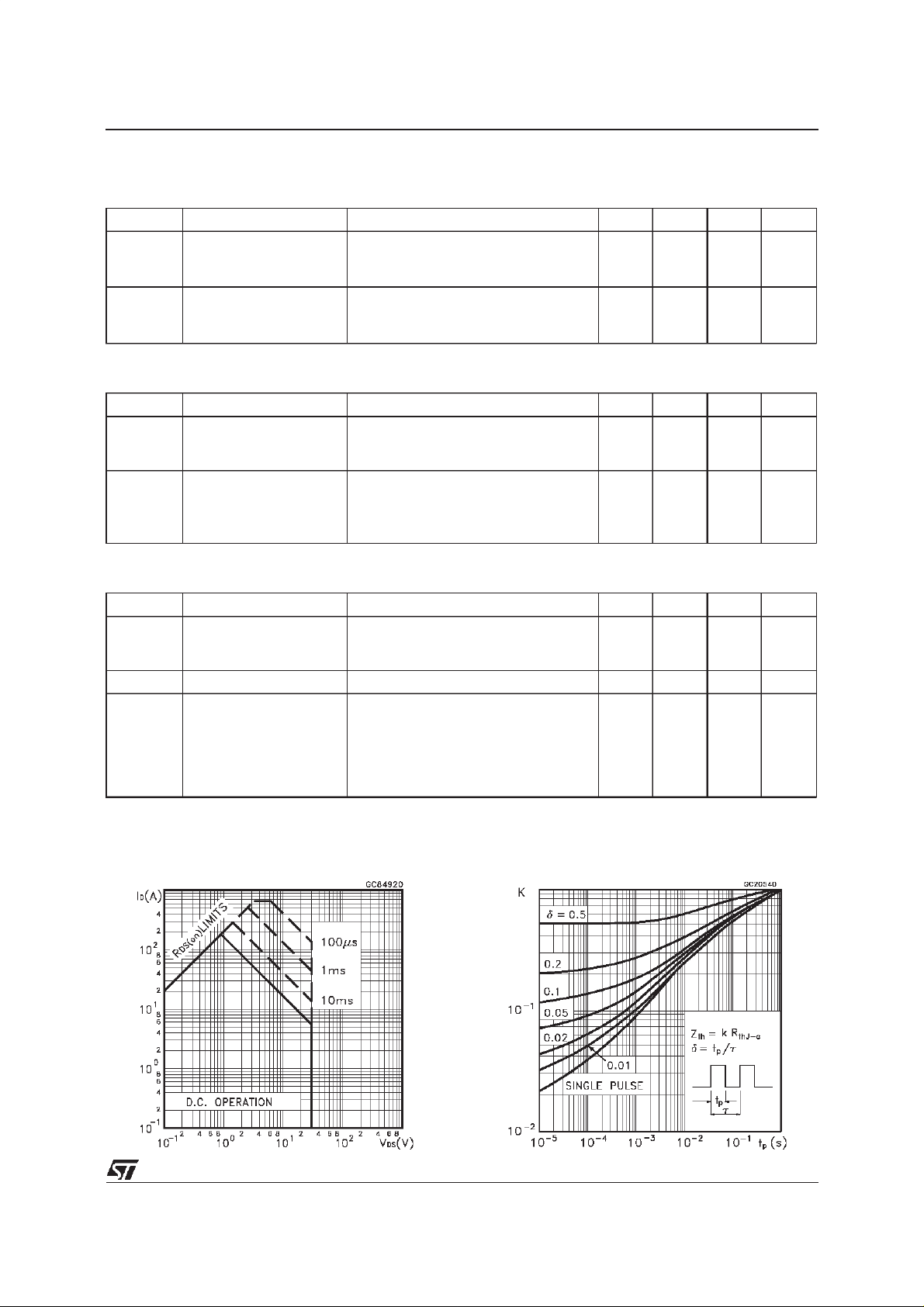
SafeOperating Area ThermalImpedance
3/8
 Loading...