

SGS Thomson Microelectronics STV0299B Datasheet
■
MULTISTANDARD QPSK AND BPSK
DEMODULATION
■
EASY IMPLEMENTATION WITH LOW COST
DIRECT CONVERSION TUNERS
■
EXTREMELY LOW BER WHEN
CO-CHANNEL INTERFERENCE
■
WIDE CARRIER LOOP TRACKING RANGE TO
COMPENSATE FOR DISH FREQUENCY DRIFT
■
COMMON INTERFACE COMPLIANT
■
VERY LOW POWER CONSUMPTION
■
INTEGRATED DUAL 6-BIT ANALOG TO
DIGITAL CONVERTERS
■
DUAL DIGITAL AGC
■
DIGITAL NYQUIST ROOT FILTER WITH
ROLL-OFF OF 0.35 OR 0.20
■
DIGITAL CARRIER LOOP WITH LOCK
DETECTOR, ON-CHIP WIDE RANGE
DEROTATOR AND TRACKING LOOP
(TYP ± 45 MHz)
■
DIGITAL TIMING RECOVERY WITH LOCK
DETECTOR
■
CHANNEL BIT RATE UP TO 90 Mbps AND
SYMBOL FREQUENCY RATE FROM
1 TO 50 MSYMBOLS
■
INNER DECODER:
- VITERBI SOFT DECODER FOR
CONVOLUTIONAL CODES, M=7, RATE 1/2
- PUNCTURED CODES 1/2, 2/3, 3/ 4, 5/6, 6/7 AND 7/8
■
SYNCHROWORD EXTRACTION
■
CONVOLUTIVE DEINTERLEAVER
■
OUTER DECODER:
- REED-SOLOMON DECODER FOR
16 PARITY BYTES; CORRECTION OF UP
TO 8 BYTE ERRORS
- ENERGY DISPERSAL DESCRAMBLER
■
ON-CHIP FLEXIBLE CLOCK SYSTEMS TO
ALLOW USE OF EXTERNAL CLOCK
SIGNALS IN 4 MHz TO 30 MHz RANGE
■
EASY-TO-USE C/N ESTIMATOR WITH 2 TO
18 dB RANGE
■
I2C SERIAL BUS AND REPEATER
■
DVB COMMON INTERFACE COMPLIANT
PARALLEL OUTPUT FORMAT
■
PARALLEL AND SERIAL DATA OUTPUT
■
LNB SU PPLY CO NTROL WITH STANDARD I/O,
22 KHz TONE AND DISEQC
TM
MODULATOR
WITH TTL OUTPUT
■
CMOS TECHNOLOGY: 2.5 V OPERATION;
JEDEC (EIA/JESD8-5)
STV0299B
QPSK/BPSK LINK IC
TQFP64
(Thin Plastic Quad Flat Pack)
ORDER CODE:
APPLICATIONS
■
DIGITAL SATELLITE RECEIVER AND
SET-TOP BOXES
DESCRIPTION
The STV0299 Satellite Receiver with FEC is a
CMOS single-chip multistand ard demodulator for
digital satellite broadcasting. It consists of two A/D
converters for I-input and Q-input, a multistandard
QPSK and BPSK demodulator, and a forward
error correction (FEC) unit having both a n inner
(Viterbi) and outer (Reed-Solomon) decoder.
The FEC unit is compliant with the DVB-S and
TM
specifications. Processing is fully digital.
DSS
It integrates a derotator before the Nyquist root
filter, allowing a wide range of offset tracking.
The high sampling rate facilitates the
implementation of low-cost, direct conversion
tuners.
A variety of configurations and beh aviours can be
selected through a bank of control/configuration
registers via an I
Transport Streams and interfaces seamlessly to
the Packet Demultiplexers embedded in ST’s
ST20-TPx or STi55xx. High sampling frequency
(up to 90MHz) considerably reduces the cost of
LPF of direct conversion tuners.
The multistandard capability associated with a
broad range of input frequency operat ions makes
it easy-to-use. Its low power consumption, small
package and optional serial output interface
makes it perfect for embedding into a tuner.
(10 x 10 x 1.4 mm)
STV0299B (
2
C. The chip outputs MPEG
No Slug)
May 2000 1/36
This is preliminary information on a new product now in development or undergoing evaluation. Details are subject to change without not i ce.

STV0299B
PageTABLE OF CONTENTS
1 PIN INFORMATION . . . . . . . . . . . . . . . . . . . . . . . . . . . . . . . . . . . . . . . . . . . . . . . . . . . . . . . . . . . . . . 4
1.1 Pin Connections . . . . . . . . . . . . . . . . . . . . . . . . . . . . . . . . . . . . . . . . . . . . . . . . . . . . . . . . . . . 4
1.2 Pinout Description. . . . . . . . . . . . . . . . . . . . . . . . . . . . . . . . . . . . . . . . . . . . . . . . . . . . . . . . . . 5
2 BLOCK DIAGRAM. . . . . . . . . . . . . . . . . . . . . . . . . . . . . . . . . . . . . . . . . . . . . . . . . . . . . . . . . . . . . . . 6
3 SYSTEM CHARACTERISTICS . . . . . . . . . . . . . . . . . . . . . . . . . . . . . . . . . . . . . . . . . . . . . . . . . . . . . 6
4 FUNCTIONAL DESCRIPTION . . . . . . . . . . . . . . . . . . . . . . . . . . . . . . . . . . . . . . . . . . . . . . . . . . . . . . 7
4.1 Front End Interfaces . . . . . . . . . . . . . . . . . . . . . . . . . . . . . . . . . . . . . . . . . . . . . . . . . . . . . . . . 7
4.2 Signal Processing . . . . . . . . . . . . . . . . . . . . . . . . . . . . . . . . . . . . . . . . . . . . . . . . . . . . . . . . . 12
4.3 Timing Recovery . . . . . . . . . . . . . . . . . . . . . . . . . . . . . . . . . . . . . . . . . . . . . . . . . . . . . . . . . . 13
4.4 Carrier Recovery and Derotator Loop . . . . . . . . . . . . . . . . . . . . . . . . . . . . . . . . . . . . . . . . . 14
4.5 Noise Indicator. . . . . . . . . . . . . . . . . . . . . . . . . . . . . . . . . . . . . . . . . . . . . . . . . . . . . . . . . . . . 14
4.6 Forward Error Correction . . . . . . . . . . . . . . . . . . . . . . . . . . . . . . . . . . . . . . . . . . . . . . . . . . . 15
5 REGISTER LIST. . . . . . . . . . . . . . . . . . . . . . . . . . . . . . . . . . . . . . . . . . . . . . . . . . . . . . . . . . . . . . . . 19
6 ELECTRICAL CHARACTERISTICS . . . . . . . . . . . . . . . . . . . . . . . . . . . . . . . . . . . . . . . . . . . . . . . . 29
6.1 Absolute Maximum Ratings . . . . . . . . . . . . . . . . . . . . . . . . . . . . . . . . . . . . . . . . . . . . . . . . . 29
2
4.1.1 I
C Interface. . . . . . . . . . . . . . . . . . . . . . . . . . . . . . . . . . . . . . . . . . . . . . . . . . . . . . . . . . . 7
4.1.2 Write Operation (Normal Mode). . . . . . . . . . . . . . . . . . . . . . . . . . . . . . . . . . . . . . . . . . . . 7
4.1.3 Read Operation (Normal Mo de). . . . . . . . . . . . . . . . . . . . . . . . . . . . . . . . . . . . . . . . . . . . 7
2
4.1.4 I
C Interface in Standby Mode . . . . . . . . . . . . . . . . . . . . . . . . . . . . . . . . . . . . . . . . . . . . . 7
4.1.5 Specific Concerns about SCL Freq uency . . . . . . . . . . . . . . . . . . . . . . . . . . . . . . . . . . . . 8
4.1.6 Identification Register. . . . . . . . . . . . . . . . . . . . . . . . . . . . . . . . . . . . . . . . . . . . . . . . . . . . 8
4.1.7 Sampling Freque nc y . . . . . . . . . . . . . . . . . . . . . . . . . . . . . . . . . . . . . . . . . . . . . . . . . . . . 8
4.1.8 Clock Generation . . . . . . . . . . . . . . . . . . . . . . . . . . . . . . . . . . . . . . . . . . . . . . . . . . . . . . . 8
4.1.9 Clock Registers . . . . . . . . . . . . . . . . . . . . . . . . . . . . . . . . . . . . . . . . . . . . . . . . . . . . . . . 1 0
4.1.10 I2C Bus Repeater . . . . . . . . . . . . . . . . . . . . . . . . . . . . . . . . . . . . . . . . . . . . . . . . . . . . . 10
4.1.11 General Purpose Σ∆DAC . . . . . . . . . . . . . . . . . . . . . . . . . . . . . . . . . . . . . . . . . . . . . . 10
4.1.12 DiSEqC Interface . . . . . . . . . . . . . . . . . . . . . . . . . . . . . . . . . . . . . . . . . . . . . . . . . . . . . 10
4.1.13 Standby Mode . . . . . . . . . . . . . . . . . . . . . . . . . . . . . . . . . . . . . . . . . . . . . . . . . . . . . . . 11
4.2.1 I and Q Inputs. . . . . . . . . . . . . . . . . . . . . . . . . . . . . . . . . . . . . . . . . . . . . . . . . . . . . . . . . 1 2
4.2.2 Main AGC (or AGC1). . . . . . . . . . . . . . . . . . . . . . . . . . . . . . . . . . . . . . . . . . . . . . . . . . . 12
4.2.3 Nyquist Root and Interpolation Filters . . . . . . . . . . . . . . . . . . . . . . . . . . . . . . . . . . . . . . 12
4.2.4 Offset Cancellation. . . . . . . . . . . . . . . . . . . . . . . . . . . . . . . . . . . . . . . . . . . . . . . . . . . . . 12
4.2.5 Signal AGC (or AGC2). . . . . . . . . . . . . . . . . . . . . . . . . . . . . . . . . . . . . . . . . . . . . . . . . . 12
4.3.1 Timing Control . . . . . . . . . . . . . . . . . . . . . . . . . . . . . . . . . . . . . . . . . . . . . . . . . . . . . . . . 13
4.3.2 Loop Equation . . . . . . . . . . . . . . . . . . . . . . . . . . . . . . . . . . . . . . . . . . . . . . . . . . . . . . . . 13
4.3.3 Timing Lock Indicator. . . . . . . . . . . . . . . . . . . . . . . . . . . . . . . . . . . . . . . . . . . . . . . . . . . 13
4.4.1 Loop Parameters . . . . . . . . . . . . . . . . . . . . . . . . . . . . . . . . . . . . . . . . . . . . . . . . . . . . . . 1 4
4.4.2 Carrier Lock Detector. . . . . . . . . . . . . . . . . . . . . . . . . . . . . . . . . . . . . . . . . . . . . . . . . . . 14
4.4.3 Derotator Frequency . . . . . . . . . . . . . . . . . . . . . . . . . . . . . . . . . . . . . . . . . . . . . . . . . . . 14
4.4.4 Carrier Frequency Offset Detector. . . . . . . . . . . . . . . . . . . . . . . . . . . . . . . . . . . . . . . . . 14
4.6.1 FEC Modes . . . . . . . . . . . . . . . . . . . . . . . . . . . . . . . . . . . . . . . . . . . . . . . . . . . . . . . . . . 15
4.6.2 Viterbi Decoder and Synchronization. . . . . . . . . . . . . . . . . . . . . . . . . . . . . . . . . . . . . . . 15
4.6.3 Synchronization . . . . . . . . . . . . . . . . . . . . . . . . . . . . . . . . . . . . . . . . . . . . . . . . . . . . . . . 16
4.6.4 Error Monitoring . . . . . . . . . . . . . . . . . . . . . . . . . . . . . . . . . . . . . . . . . . . . . . . . . . . . . . . 16
4.6.5 Convolutional Deinterleaver. . . . . . . . . . . . . . . . . . . . . . . . . . . . . . . . . . . . . . . . . . . . . . 16
4.6.6 Reed-Solomon Dec oder and Desc ramb ler . . . . . . . . . . . . . . . . . . . . . . . . . . . . . . . . . . 16
4.6.7 Parallel Output Interface . . . . . . . . . . . . . . . . . . . . . . . . . . . . . . . . . . . . . . . . . . . . . . . . 16
4.6.8 Serial Output Interface. . . . . . . . . . . . . . . . . . . . . . . . . . . . . . . . . . . . . . . . . . . . . . . . . . 17
2/36

STV0299B
(continued)
PageTABL E OF CONTENTS
6.2 Thermal Data . . . . . . . . . . . . . . . . . . . . . . . . . . . . . . . . . . . . . . . . . . . . . . . . . . . . . . . . . . . . . 29
6.3 DC Electrical Characteristics. . . . . . . . . . . . . . . . . . . . . . . . . . . . . . . . . . . . . . . . . . . . . . . . 29
6.4 Timing Characteristics . . . . . . . . . . . . . . . . . . . . . . . . . . . . . . . . . . . . . . . . . . . . . . . . . . . . . 31
2
C Bus Characteristics. . . . . . . . . . . . . . . . . . . . . . . . . . . . . . . . . . . . . . . . . . . . . . . . . . . . . 32
6.5 I
7 APPLICATION BLOCK DIAGRAMS. . . . . . . . . . . . . . . . . . . . . . . . . . . . . . . . . . . . . . . . . . . . . . . . 33
8 PACKAGE MECHANICAL DATA . . . . . . . . . . . . . . . . . . . . . . . . . . . . . . . . . . . . . . . . . . . . . . . . . . 35
3/36
STV0299B
1 PIN INFORMATION
1.1 Pin Connections
Figure 1:
Pinout for 64-pin TQFP (10x10 mm)
CLK_IN/XTAL_IN
XTAL_OUT
V
AUX_CLK
V
DD_3.3V
RESET
F22/DiSEqC
V
SSA
DDA
V
SS
V
DD
V
SS
AGC
V
DD
V
SS
SDA
SCL
SS
DD
V
V
64 62 61 60 59 58 57 56 5563 54 53 52 51 50 49
1
2
3
4
5
6
7
8
9
10
11
12
13
14
15
16
17 19 20 21 22 23 24 25 2618 27 28 29 30 31 32
TEST
TEST
SDAT
SCLT
SSA
V
DIRCLK-DIS
DDA
TOP
V
QP
V
QN
SSA
V
IN
IP
SSA
V
V
48
47
46
45
44
43
42
40
39
38
37
36
35
34
33
41
BOT
V
DDA
TEST
TEST
TEST
TEST
STDBY
V
DD
DAC
V
SS
IP0
TEST
D0
D1
D2
D3
4/36
V
SS
D6
D5
V
DD
STR_OUT
SS
V
DD_3.3 V
V
CLK_OUT
OP1
OP0
D/P
ERROR
LOCK/OP2
D4
SS
V
SERIAL DATA/D7
STV0299B
1 PIN INFORMATION
(continued)
1.2 Pinout Description
Pin Number Name
SIGNAL INPUTS
50, 51 IP, IN I Analog in Phase Component
53, 54 QN, QP I Analog in Quadrature Component
1 CLK_IN/XTAL IN I Crystal Input or CLK_IN
2 XTAL OUT O Crystal Output
9AGC
5 AUX_CLK
17-18 OP0, OP1
19 LOCK/OP2
38 IP0 I Input Port
SIGNAL OUPUTS
26-28-29-31, 33 to 36 D[7:0]
24 CLK_OUT
22 STR_OUT
21 D/P
20 ERROR
14 SCL
12 SDA
OTHERS
59 SCLT
60 SDAT
37-43-44-45-46-61-62 TEST I
58 DIRCLK_DIS I
3, 49, 52, 57
4, 47, 55
56
48
6-8-11-23-27-32-39-64
13-25
7-10-30-41-63
15 RESET
42 STDBY I Sets STDBY at power on
16 F22/DiSEqC
40 DAC
Note: 1
The following abbreviations are used: I - Input; O - Output; OD - Open drain output.
2
3.3 V outpu t levels.
3
5 V tolerant
V
SSA
V
DDA
V
TOP
V
BOT
V
SS
V
DD_3.3 V
V
DD
1
I/O
FRONT END CONTROLS
3
Control Signal to the Tuner
OD
2
Programmable Output Port or Programmable Output Clock
O
2
Programmable Output Ports
O
2
Carrier Found or Data Found or Output Port
O
2
Output Data; D7 is DATA_OUT in Serial Mode
O
2
Output Byte Clock; or Bit Clock in Serial Mode
O
2
Output 1st byte Signal (synchro byte clock)
O
2
Data/Parity Signal
O
2
Output Error Signal. Set in case of uncorrectible packet.
O
I2C INTERFACE
3
Serial Clock (I2C bus)
I
3
I/OD
Serial Data (I2C bus)
3
Tuner Serial Clock (repeator) or Output Port
OD
3
Tuner Serial Data (repeator) or Input/Output Port
I/OD
Reserved for manufacturing tests; must be tied to V
Sets the DIRCLK function at power on
S Analog Ground
S Analog 2.5 V Supply
S ADC High Voltage Reference
S ADC Low Voltage Reference
S Ground
S 3.3 V Supply
S 2.5 V Supply
I Reset, active at low level
DiSEqC modulation, 22 kHz Tone, Programmable
2
O
Output Port
2
Programmable Digital to Analog Converter Output
O
Description
SS
5/36

STV0299B
-
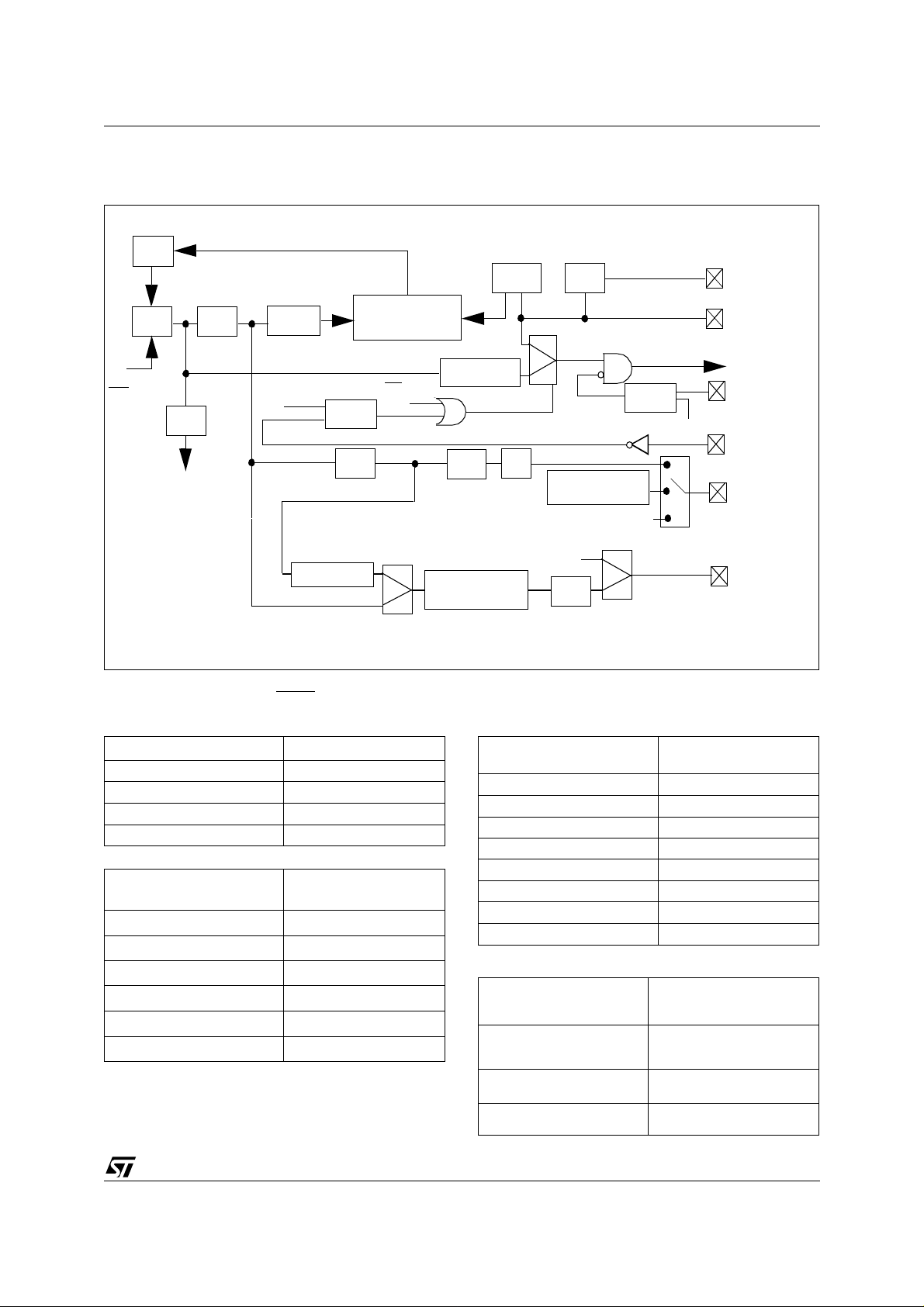
2 BLOCK DIAGRAM
AGC
V
DDA
V
TOP
IN/IP
QN/QP
V
BOT
V
SSA
CLK_IN/XTAL_IN
AUX_CLK
Nyquist &
Interpolation
Filter
Derotator
AGC1
Offset
Comp.
ADCs
Clock
Generator
AGC2
Carrier Lock
Indicator
Error
Monitoring
Timing
Recovery
Timing
DCO
Timing
Lock
Indicator
C/N
Indicator
Viterbi Decoder
Deinterleaver
XTAL_OUT
F22/DiSEqC
SCL
SDA
22 kHz
Tone
DiSEqC
Interface
2
I
C
Interface
SDAT SCLT DAC IP0 OP0[2:0] D[7:0] V
General
Purpose
Functions
3 SYSTEM CHARACTERIST ICS
Performances
The following given parameters are for indication
purposes only.
Carrier Loop Tracking Range:
M_CLK
/2
• ±f
Carr i er Loop Ca pt ure Range ( C / N>=4 dB):
• up to ± 5% fs in less than 100 Ksymbols
• up to ± 2% fs in less than 10 Ksymbols
C/N Threshold (lowest C/N at which capture is
possible) = 1 dB.
Reed-Solomon
Decoder
D/P
Energy
Descrambler
DD_3.3VVDDVSS
ERROR
STR_OUT
CLK_OUT
Timi ng Loop Capt ure Range (C/N>=2 dB ):
• up to ±250 ppm in less than 100 Ksymbols
• conventions used for the above characteristics
are:
f
sampling
fs = f
C/N = Carrier/Noise =
PR = Puncture Rate
= f
symbol
m_clk
= f
master_clock
Eb
------ -x2xPR
No
6/36
4 FUNCTIONAL DESCRIPTION
STV0299B
The STV0299B is a multistandard demodulator
and error correction decoder IC for the reception
of QPSK and BPSK modulated signals. It is
intended for use in digital satellite television
applications. The IC can accept two standards of
QPSK modulated signals (DVB and DSS) as well
as BPSK modulated signals over a wide symb ol
frequency range (from 1 to 50 Msymbol s/s). The
signals are digitized via an integrated dual 6-bit
analog to digital converter, and interpolated and
digitally filtered by a Nyquist root filter (with a
settable roll-off value of either 0.35 or 0.20).
There are two built-in digital Automatic Gain
Controls (AGCs). The first AGC allows the tuner
gain to be controlled by the pulse density
modulated output. The second AGC performs
power optimization of the digital signa l bandwidth
(internal to the STV0299B). The digital signal then
passes through the digital carrier loop fitted with
an on-chip derotator and tracking loop, lock
detector, and digital timing recovery.
Forward error correction is integrated by way of an
4.1.2 Write Operation (Normal Mode)
The byte sequence is as follows:
1 The first byte gives the device address plus the
direction bit (R/W = 0).
2 The second byte contains the internal address
of the first register to be accessed.
3 The next byte is written in the internal regist er.
Following bytes (if any) are written in
successive internal registers.
4 The transfer lasts until stop conditions are
encountered.
5 The STV0299B acknowledges every byte
transfer.
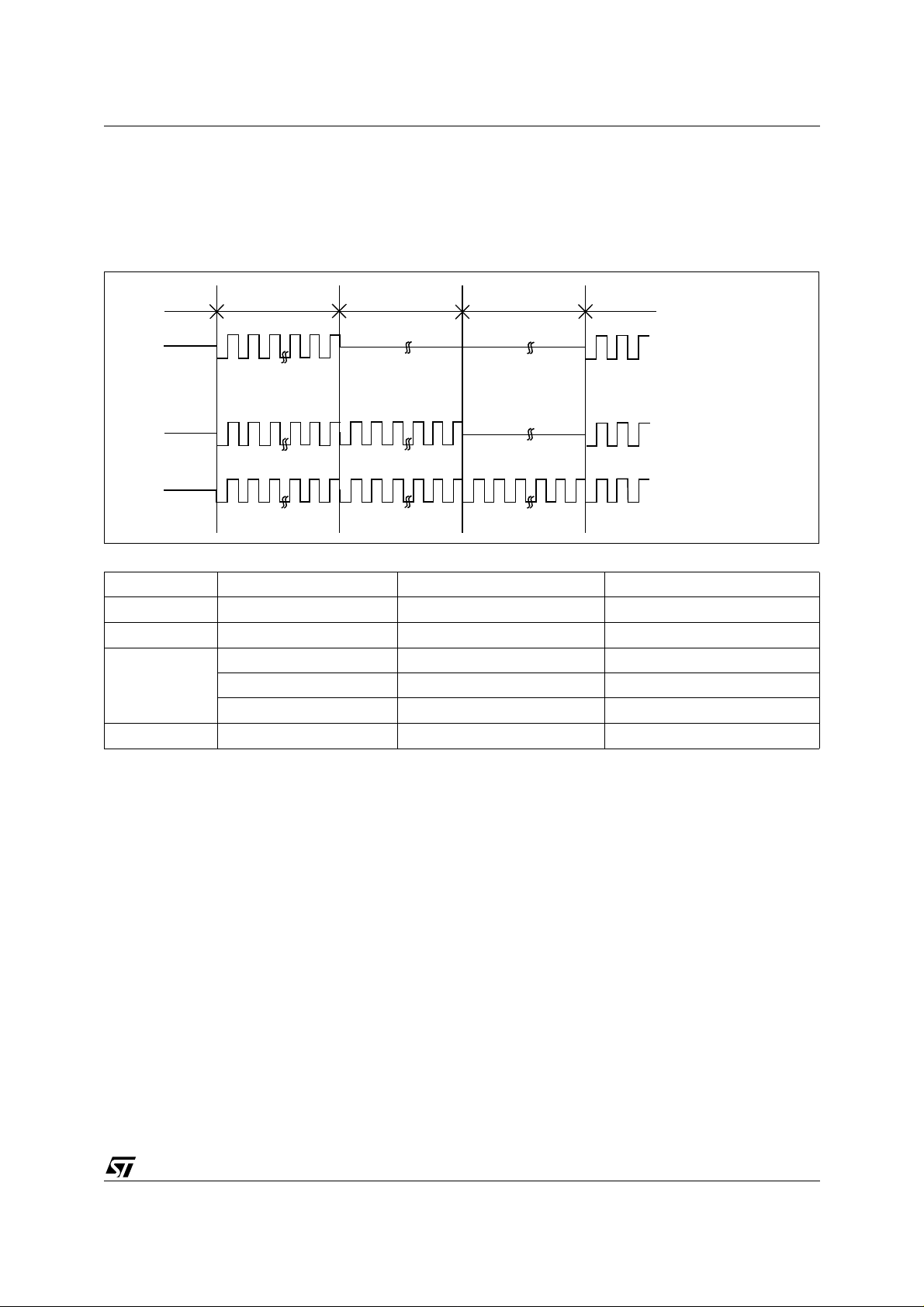
4.1.3 Rea d Op e rat i on (N ormal Mode )
The address of the first register to read is
programmed in a write operation without data, and
terminated by the stop condition. Then, another
start is followed by the device address and R/
W = 1. All following bytes are now data to be read
at successive positions starting from the initial
address. Figure 2 shows the I
2
C Normal Mode
Write and Read Registers.
inner Viterbi soft decoder, and an outer
Reed-Solomon decoder.
4.1 Front End Interfaces
2
4.1.1 I
The standard I
first byte is Hex D0 fo r a write operation, or Hex
D1 for a read operation. The I
C Interface
2
C protocol is used whereby the
2
C interface
operates differently depending on whether it is in
normal or standby mode.
4.1.4 I
Only three registers can be addressed while in
standby mode: RCR (address 01 Hex), MCR
(address 02 Hex) and ACR (address 03 Hex).
These three registers can be either read or written
to (refer to Figure 3).
Only one register may be read or written to per
sequence (no increment). While in standby mode,
the Serial Clock (SCL) frequency must be lower than
one tenth of the CLK_IN frequency (f
Figure 2:
Write registers 0 to 3 with AA, BB, CC, DD
Start
Read registers 2 and 3
Start Device Address, Write D 0 ACK Register Address 02 ACK Stop
Start
Figure 3:
Write operation
Star t Device A ddress, Wri te D0 ACK Register Address 01, 02 or 03 ACK Data ACK Stop
2
I
C Read and Write Operations in Normal Mode
Device
Address,
Write D0
2
I
C Read and Write Operations in Standby Mode
ACK
Device Address,
Read D1
Register
Address 00ACK
ACK Data Read CC ACK Data Read DD
Data
AA
ACK
2
C Interface in Standby Mode
Data
BB
ACK
Data
CC
ACK
Data
DD
CLK_IN
/ 10).
ACK Stop
ACK
Stop
Read operation
Start
Start
Note: 1
ACK is not absolutely necessary after Data
Device Address
, Read D0
Device Ad dress,
Read D1
ACK Regis ter Address ACK Stop
ACK Reader Data
ACK (or no
ACK
Stop
1
)
7/36

STV0299B
N
4 FUNCTIONAL DESCRIPTION
(continued)
4.1.5 Specific Concerns about SCL
Frequency
For reliable operation in Normal Mode, the SCL
frequency must be lower than 1/40 of the Ma ster
Clock (M_CLK) frequency. Consequently, care
should be taken to observe the following:
1 Before returning t o No rm al Mode from Sta ndby
Mode, the M_CLK frequency must be s elected
≥
such that f
M_CLK
40 f
SCL
2 After Power-on reset signal, the STV0299B
operates in Normal Mode. There are two possible cases:
- DIRCLK-DIS (pin 58) is grounded.
M_CLK = CLK_IN, the f
2
I
C bus must satisfy:
- DIRCLK-DIS (pin 58) is tied to V
100
(where ), and the f
f
M_CLK
--------- -
=
16
frequency of the
SCL
CLK_IN
f
≤
-------------------- -
SCL
f
⋅
CLK_I
40
.
DD
SCL
frequency of the I2C bus must satisfy:
f
SCL
16 40
CLK_IN
⋅≤
×
and
f
SCL
≤
400 kHz.
100
-------------------
For example, this second operating mode is
required when the app lication features both a
4 MHz XT AL and a 400 kHz I
2
C bus.
4.1.6 Identification Register
The Identification Register (at address Hex 00)
gives the release number of the circuit.
The content of this register at reset is presently A1
(same as STV0299).
4.1.7 Sampl i ng Frequency
The STV0299B converts the analog inputs into
digital 6-bit I and Q flows. The sampling frequency
is f
reference described in Section 4.1.8
Generation’
which is derived from an external
M_CLK
. The maximum value of f
‘Clock
M_CLK
is 90
MHz.
The sampling causes the repetition of the input
spectrum at each integer multiple of f
M_CLK
. One
has to ensure that no frequency component is
folded in the useful signal b andwidth of f
where f
is the symbol frequency, and α is the
S
(1+α)/2
S
roll-off value.
4.1.8 Clock Generation
An integrated VCO (optimised to r un in the range
of 300 to 400 MHz) is locked to a reference
frequency provided by a crystal o scillator by the
following relation:
M1
+
f
VCOfref
4M1
==
()⋅⋅
f
+
XTAL
4
⋅⋅
--------------
K1
+
The VCO’s loop filter is optimized for a reference
frequency between 4 and 8 MHz.
The VCO generates the following by division:
• The Master Clock (M_CLK)
• An auxiliary clock (AUX_CLK) which may either
be in the MHz range or in the 25 Hz to 1500 Hz
range for some specific LNB control (for
example, 60 Hz).
• A lower frequency, F22, typically 22 KHz,
needed for LNB control or DiSEqC
TM
control.
When DIRCLK_CTRL = 1, the crystal signal is
routed directly to M_CLK; the VCO may still be
used to generate AUX_CK and/or the F22 (used
by the DiSEqC
TM
int erface).
If the internal VCO is not used by any of the
dividers, it may be stopped in order to decrease
the power consumption and/or radiation
emissions. The only guaranteed function in
standby mode is the I
2
C Write/Read function of
the three clock control registers.
There are restrictions on the high and low level
durations, and on the crystal (or external clock)
frequency when the direct clock is used.
These restrictions are explained in Section 4.1.5
Specific Concerns about SCL Frequency
.
8/36
STV0299B
)
]
]
]
]
g
4 FUNCTIONAL DESCRIPTION
Figure 4:
Clock Signal Generation
LPF
Reg 01[4:0
VCO 1/4
VCO
/OFF
ON
TO SERIAL
SHIFTER
1/6
÷(M+1)
I2C
Note 2
PRESCALER
(continued)
PHASE
COMPARATOR
VCO ON/OFF
DIRCLK (I2C bit
1/16
÷(K+1) OSC
Reg 02[2:0
÷P(Note 1)
DIRCLK-CTRL
÷R
Reg 04
PROGRAMABLE
DIVIDER
Reg 01[7:6
1
0
1/2
2
C bit)
Note 2
STDBY
(I
DiSEqC/tone
burst modulator
1/0
1/0
1/2
03
Re
Reg 08[2:0
XTAL OUT
XTAL IN/CLK-IN
M_CLK
STDBY
I2C
DIRCLK-DIS
F22/
DiSEqC
AUX_CLK
TM
Note: 1
Refer to the Re gi ster List P[2:0] in table 1
2
At the rising edge of RESET signal (pin 15) the corresponding bit of the I2C bus register is forced to the status of pin STDBY or
to DIRCLK -DIS.
Table 1:
K(1:0) in register
M(4:0) in register
f
REF
= f
XTAL
Divider Programming
00 1
01 2
10 3
11 4
= f
f
VCO
multiplied by:
00000 4
00001 8
00010 12
00011 16
... ...
11111 128
divided by:
REF
P(2:0) in register
Table 2:
f
=
VCOfXTAL
f
M_CLK
f
=
M_CLKfCLK_IN
f
M_CLK
f
M_CLK
divided by P:
000 4
001 6
010 8
011 12
100 16
101 24
110 32
111 48
Summary of F
M1
4
⋅×
--------------
K1
f
VCO
----------- -=
P
M_CLK
+
+
DIRCLK_CTRL = 0
DIRCLK_CTRL =1
0
=
STDBY = 1
= f
VCO
9/36

STV0299B
4 FUNCTIONAL DESCRIPTION
(continued)
4.1.9 Clock Registers
The Reference Clock, Master Clock, Auxiliary
Clock and F22 Frequency Registers are in
Addresses 01, 02, 03 and 04.
2
4.1.10 I
In low symbol rate applications, signal pollution
generated by the SDA/SCL lines of the I
C Bus Repeater
2
C bus
may dramatically worsen tuner phase noise. In
order to avoid this problem, the STV0299B offers
2
C bus repeater so that the SDAT and SCLT
an I
are active only when necessary and muted once
the tuner frequency has settled.
Both SDAT and SCLT pins are set high at reset.
When the microprocessor writes a 1 into register
2
CT, the next I2C message on SDA and SCL is
bit I
repeated on the SDAT and SCL T pins respectively,
until stop conditions are detected.
To write to the tuner, the external microprocessor
must, for each tuner message, perform the
following:
2
• Program 1 in I
CT.
• Send the message to the tuner.
Any size of byte transfers are allowed, regardless
of the address, until the stop conditions are
detected. Transfers are fully bi-directional.
2
CT bit is automatically reset at the stop
The I
condition. If not used for the I
2
C repeater, both
SDAT and SCLT outputs may be used as general
purpose output por t s.
SDAT status may be read on the DiSEqC register.
Configuration is controlled by the I
2
C repeater
register in Address 0Ah.
In the first version of the STV0299, operation of
the repeater was very fast, and often too fast
versus the rise time of the SDAT and SCLT
signals. In the STV0299B, a programmable delay
is implemented to accept a wide range of rise
times on SDAT and SCLT. The delay is
programmed with Reg.05 [5:4]. In practice,
operation of the repeater is ensured in the
following case:
• Reg.05 [5:4]: xx
≤
• f
M_CLK
90 MHz
• RC≤250ns (R: pull-up resistor, C: total
capacitance on either SDAT or SCLT).
4.1.11 Gener al Purp ose Σ∆DAC
A DAC is available in order to control external
analog devices. It is built as a sigma-delta
first-order loop, and has 12-bit resolution-it only
requires an external low-pass filter (simple RC
filter). The clock frequency is derived from the
main clock by programmable division. The
converter is controlled by two registers-one for
clock divider control and 4 MSBs, and the other for
the 8 LSBs.
If the DAC is not needed, the DAC output may be
used as an output por t . The DAC Registers are in
Addresses 06 and 07.
4.1.12 DiSEqC Interface
This interface allows for the simplification of real
time processing of the dialog from microprocessor
to LNB. It includes a FIFO that is filled by the
microprocessor via the I
2
C bus, and then
transmitted by modulating the F22 clock adjusted
beforehand to 22 kHz.
2
Two control signals are available on the I
C bus:
FE (FIFO empty) and FF (FIFO full).
A typical byte transfer loop, as seen from the
microprocessor, may be the following:
While (there is data to transfer)
1 Read the control signals
2 If FF=1, go to 1
3 Write byte to transfer in the FIFO
Note, for the above transfer loop, the following:
• At the beginning, the FIFO is empty (FE=1,
FF=0). This is the idle state.
• As soon as a byte is written in the FIFO, the
transfer will begin.
• After the last transmitted byte, the interface will
go into the idle state.
Modulation
The output is a gated 22 kHz square signal.
In the idle state
•
, modulation is permanently
inactive.
In byte transmission
•
, the byte is sent (MSB
first) and is followed by an odd parity bit.
A byte transmission is therefore a serial 9-bit
transmission with an odd number of “1’s”.
Each bit lasts 33 periods of F22 and the
transmission is PWM-modulated.
Transmission of “0’s”
-
. There are two
submodes controlled by PortCtrl(2):
a) PortCtrl2 = 1: Modulation is active during
22 pulses, then inactive during 11 pulses
(2/3 PWM ) .
b) PortCtrl2 = 0: Modulation is active during
33 pulses (3/3 PWM).
Transmission of “1’s”
-
. During transmission
of “1’s”, modulation is active during 11 pulses,
then inactive during 22 pulses (1/3 PWM).
This is com patible w ith “Tone Burst” in older LNB
protocols.
For the “Modulated Tone Burst”, only one byte
(with value Hex FF) is written in the FIFO.
The parity bit is 1, and as a result, the output
signal is 9 bursts of 0.5 ms, separated by
8 intervals of 1 ms.
10/36
STV0299B
For t he “Unmodulated Tone Burst” Port C TRL 2 is
set to 0 and, only one byte, of value 00h is sent.
The parity bit is still 1, and as a r esult, the signal is
a continuous train of 12.5 ms. When the
alternatively to VDD and VSS levels. The DiSE qC
and Lock Control, DiSEqC FIFO and DiSEqC
Status Registers are in Addresses 08, 09 and
0Ah.
modulation is active, the DiSEqC output is driven
Figure 5:
Schematic showing Bit Transmiss ion
Idle 11 Periods 11 Periods 11 Periods Next bit
Transmission of 1’s
Transmission of 0’s:
a) PortCtrl2 = 1
b) PortCtrl2 = 0
Table 3:
PortCtrl (1:0) PortCtrl (2) FIFO Output
00 X empty 0
01 X empty 1
0 DATA = 00 Unmodulated tone burst
1 DATA = FFor00 Modulated tone burst
1 Note 1 DiSEqC signal
Note: 1
10
11 X XX Continuous tone
Byte to transfer in DiSEqC mode.
2
In mode PortCtrl (1:0)=10, the F22/DiSEqC pin returns to High -2 mode once the transmission is completed.
4.1.13 Standby Mode
A low power consumption mode (standby mode)
can be implemented (in this mode, f
standby mode, the I
2
C decoder still operates, but
with some restrictions (see Sections
4.1.5
).
Standby mode can be initiated or stopped by I
M_CLK
4.1.4
= 0). In
and
2
bus commands as described in MCR Register 02.
At power-on, the circuit starts to operate in
standby mode when the STDBY pin (pin 42) is
tied to V
. This guarantees low power
DD
consumption for the stand-alone modules
(PCMCIA size front-end modules) before any
command is initiated. After the power-on
C
sequence, the standby mode is entirely controlled
via MCR Register (02).
11/36
 Loading...