

SGS Thomson Microelectronics STV0196B Datasheet
STV0196B
QPSK/BPSK DEMODULATOR AND FEC IC
FRONT-END INTERFACE
.
I AND Q6 BITSDIGITALINPUTS AT2Fs
.
QPSKDEMODULATION(TwoModes: A andB)
.
INPUT SYMBOL FREQUENCY (Fs) UP TO
30MSYMBOLS/S
.
DIGITALNYQUIST ROOT FILTER:
ROLL-OFF VALUEOF 0.35IN MODEA
.
DIGITALCARRIER LOOP:
- ON-CHIP DEROTATOR AND TRACKING
LOOP
- CARRIER OFFSETINDICATOR
- LOCKDETECTOR
- C/NINDICATOR FOR DISH POSITIONING
.
DIGITALTIMING RECOVERY :
- INTERNAL TIMING ERROR EVALUATION
AND FILTER
- OUTPUT CONTROL SIGNAL FOR A 2Fs
EXTERNALVCO OR VCXO
.
DIGITALAGC :
- INTERNAL SIGNAL POWER ESTIMATION
AND FILTER
- OUTPUT CONTROLSIGNAL FOR AGC
(1 BIT PULSE DENSITYMODULATION)
FORWARD ERROR CORRECTION
.
INNERDECODER :
- VITERBISOFT DECODER FORCONVOLUTIONAL CODES, CONSTRAINT LENGTH
M = 7, RATE1/2
- PUNCTURED CODES 1/2, 2/3,3/4, 5/6 AND
7/8 INMODE A
- AUTOMATI C OR MANUAL RATE AND
PHASERECOGNITION
.
DEINTERLEAVER :
- WORDSYNCHRO EXTRACTION
- CONVOLUTIVEDEINTERLEAVER
.
OUTERDECODER :
- IN MODE A : REED-SOLOMON DECODER
FOR 16 PARITYBYTES ; CORRECTIONOF
UP TO 8 BYTE ERRORS
- BLOCKLENGTHS : 204 IN MODEA
- ENERGYDISPERSALDESCRAMBLER
CONTROL
.
I2C SERIAL BUS
DESCRIPTION
Designed for the fast growing direct broadcast
sat e llite (DBS ) digital TV re ceiver market,
the SGS-THOMSON STV0196B Digital Satellite
Receiver Front-end integrates all the functions
neededtodemodulateincomingdigital satellite TV
signalsfromthe tuner: Nyquistfilters,QPSK/BPSK
demodulator, signal power estimator, automatic
gain control, Viterbidecoder,deinterleaver,ReedSolomon decoder and energy dispersal descrambler. This high level of integrationgreatly reduces
the package count and cost of a settop box. The
demodulator blocks are suitable for a wide range
of symbolrateswhiletheadvancederror correction
functionsguaranteealowerrorrateevenwithsmall
receiverantennas or low powertransmitters.
The STV0196Bhas multistandard capability.
It is fullycompliant with the recently definedDigital
Video Broadcasting (DVB) standard (already
adopted by satellite TV operators in the USA,
Europe and Asia) and also compatible with the
mainconsumerdigitalsatelliteTVstandardsinuse.
PQFP64
(Plastic Package)
ORDER CODE : STV0196B
September 1996
1/23
STV0196B
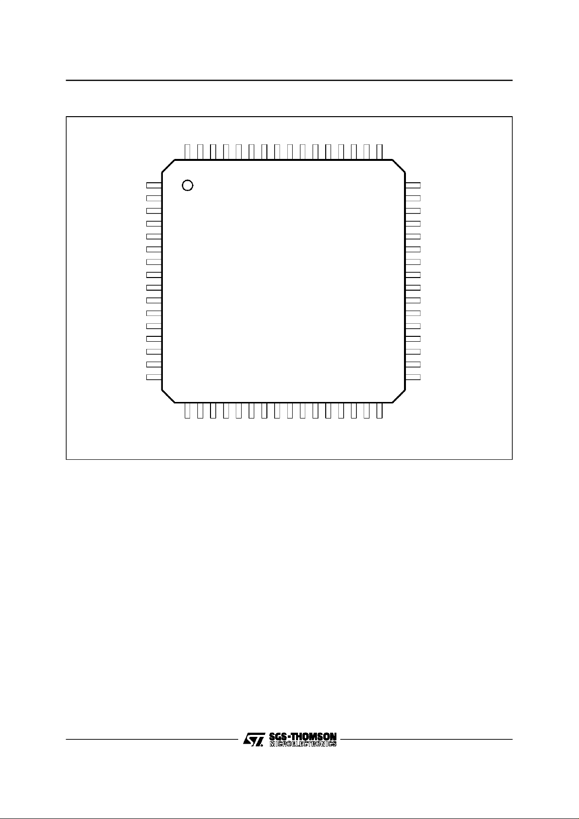
PINCONNECTIONS
TEST
V
V
TEST
TEST
V
V
V
V
V
V
TEST
TEST
TEST
TEST
TEST
TEST
Q0Q1Q2Q3Q4Q5I0
I1
I2
I3
DD
I4
VSSV
I5
64 63 62 61 60 59 58 57 56 55 54 53 52 51 50 49
1TEST
2
SS
DD
3
4
5
6
SS
DD
SS
DD
SS
DD
7
8
9
10
11
12
13
14
15
48
47
46
45
44
43
42
41
40
39
38
37
36
35
34
3316
M_C LK
MODE
CLKREC
V
DD
AGC
V
DD
V
SS
V
SS
SDA
SCL
V
DD
V
SS
NRES
D60
ERROR
D/P
17 18 19 20 21 22 23 24 25 26 27 28 29 30 31 32
D0D1D2D3D4D5D6
TEST
TEST
D7
SS
DD
V
V
CK_OUT
DD
V
STR_OUT
SS
V
0196B-01.EPS
2/23
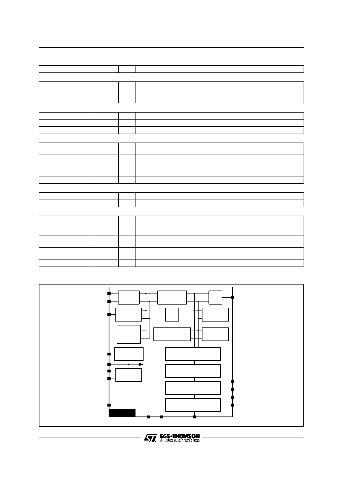
PIN LIST
Pin Number Pin Name Type Pin Description
SIGNAL INPUTS
51, 52, 53, 54, 55, 56 I [5..0] I In Phase Component, at twice the symbol frequency (2Fs).
57, 58, 59, 60, 61, 62 Q [5..0] I In Quadrature Component, at twice the symbol frequency (2Fs).
48 M_CLK I Master Clock Input,2Fs. Sampling Clock ofthe External A toD Converters.
FRONT END CONTROLS
46 CLKREC O 1 BitControl Signal for the External CLK VCO.Itmust be Low-passFiltered.
44 AGC O 1 Bit Control Signal for the External AGC. It must be Low-passFiltered.
35 D60 O M_CLK Divided by 60
SIGNAL OUTPUTS
26, 25, 24,23,
22, 21, 20,19
29 CK_OUT O Output Byte Clock
30 STR_OUT O Output Synchronization Byte Signal
33 D/P O Data/Parity Signal
34 ERROR O Output Error Signal. Set in Case of uncorrected Block.
2
C MICRO INTERFACE
I
39 SCL I Serial Clock
40 SDA I/O Serial Data Bus
OTHER
47 MODE I 0 =Mode A, 1 = ModeB
1, 2, 5, 6, 13, 14, 15,
16, 17, 18, 63, 64
3, 7, 9, 11, 28, 32,
37, 41, 42,49
4, 8, 10, 12, 27,
31, 38, 43, 45, 50
36 NRES I NegativeReset
D [7..0] O Output Data
TEST O Reserved for Manufacturing Test. Itmust remain unconnected
V
SS
V
DD
I Ground References
I 3.3V Supply
STV0196B
0196B-01.TBL
BLOCK DIAGRAM
I[5...0]
Q[5...0]
CLKREC
D60
M_CLK
SCL
SDA
MODE
NYQUIST
FILTER
TIMING
RECOVERY
CARRIER
OFFSET
MEASURE
DIVIDEBY 60
2
C BUS
I
INTERFACE
STV0196B
DEROTATOR AGC
DCO
CARRIERPHASE
TRACKINGLOOP
VITERBI DECODER
DEINTERLEAVER
REED SOLOMON DECODER
ENERGYDESCRAMBLER
V
DDVSS
D[7..0]
LOCK
INDICATOR
C/N
INDICATOR
AGC
D/P
ERROR
STR_OUT
CK_OUT
0196B-02.EPS
3/23
STV0196B
FUNCTIONAL DESCRIPTION
2
I-I
C BUS SPECIFICATION
This is the standardI
The deviceaddress is ”1101000” ; the first byte is thereforeHex D0 for a write operation and Hex D1for a
read operation.
I.1 - Write Operation
The firstbyte is thedevice address plus the directionbit (R/W = 0).
The secondbyte containsthe internaladdress of the first registerto be accessed.
The nextbyte is written in the internal register.
The following(if any)bytes arewritten in successiveinternal registers.
The transferlasts until stop conditions are encountered.
The STV0196Backnowledgeseverybyte transfer.
I.2 - ReadOperation
The addressof the first register to readis programmed in a write operation without data, and terminated
by stop condition.
Then anotherstart is followed bythe device address andR/W= 1 ; allsuccessive bytesarenowdata read
at successivepositions starting from the initial address.
The STV0196Backnowledgeseverybyte transfer.
Example :
Write registers 0 to 3 withAA,BB,CC,DD
2
C protocol.
Start
Device Address,
Write D0
ACK
Internal
Address
ACK
Data
AA
ACK
Data
BB
ACK
Data
CC
ACK Stop
Read registers 2 and3
Start
Start
Device Address,
Device Address,
Write D0
Read D1
ACK
ACK RegisterAddress 01 ACK Stop
Data Read
BB
ACK
Data Read
CC
ACK Stop
I.3 - IdentificationRegister
This read only register gives the releasenumber of the circuit in order to ensuresoftware compatibility.
The readvalue is Hex 83 for STV0196Band Hex 81 for STV0196.
Internal Address : Hex 0B
10000011
Notes : - Unspecified register addresses mustnot be used.
- Allthe unused bits in the registers must be programmed to 0.
4/23
FUNCTIONAL DESCRIPTION (continued)
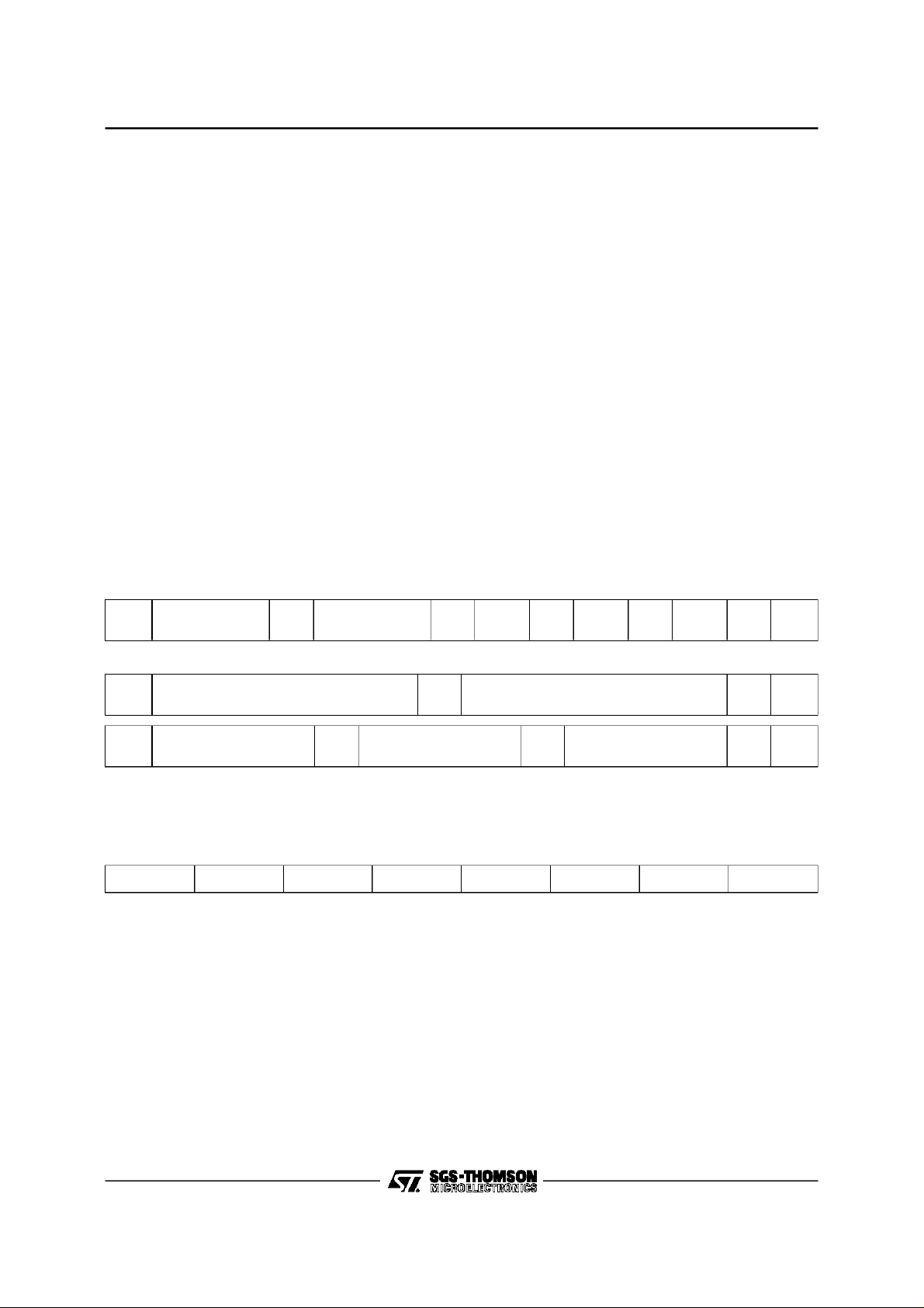
I.4 - RegisterMap
REGISTERHEX 00
INPUTCONFIGURATION REGISTER (R/W)
Reset Value : Hex04
0 -Q(1)or Q(0) input
1 Signed(1)or positive(0) I & Q inputs
2 Nyquistfilteringon (1)/ off (0)
3 BPSK(1), QPSK(0)
4 To be set to 0.
5 To be set to 0.
6 To be set to 0.
7 To be set to 0.
REGISTERSHEX 01 TO HEX 05
VITERBI,PUNCTURERATETHRESHOLDS(R/W)
Reset Value : Hex20
rate
Hex01 VTH0 0 Th6 Th5 Th4 Th3 Th2 Th1 Th0 1/2
Hex02 VTH1 0 Th6 Th5 Th4 Th3 Th2 Th1 Th0 2/3
Hex03 VTH2 0 Th6 Th5 Th4 Th3 Th2 Th1 Th0 3/4
Hex04 VTH3 0 Th6 Th5 Th4 Th3 Th2 Th1 Th0 5/6
Hex05 VTH4 0 Th6 Th5 Th4 Th3 Th2 Th1 Th0
7/8
or
6/7
REGISTERHEX 06
VSEARCH(VITERBI)(R/W)
Reset Value : Hex19
0
H[1..0] Sync counter hysteresis value
1
2
T[1..0] Syncsearch time out
3
4
5
SN[1..0]
VITERBIerrorrateaveragingperiod.
C/Nindicator averaging period.
6 F VITERBIoperatingstatusfreeze (1)
7 A/M (0) automatic,(1)manual
REGISTERHEX 07
VERROR REGISTER(Readonly)
STV0196B
REGISTERHEX 08
VSTATUSREGISTER(Read only)
0
PR[2..0] Currentpuncture rate identification
1
2
3 LK (1) synchrofound,
(0) searchingpuncture rate
4 PRF (1) puncturerate found,
(0) searchingpuncture rate
5 unused set to (0)
6 unused set to (0)
7 CF (1)carrierfound,(0)searchingcarrier
REGISTERHEX 09
PUNCTURE RATEENABLE(R/W)
ResetValue: Hex 10 (modeA)
0 E0 (1) Puncture1/2 enabled,(0) disabled
1 E1 (1) Puncture2/3 enabled,(0) disabled
2 E2 (1) Puncture3/4 enabled,(0) disabled
3 E3 (1) Puncture5/6 enabled,(0) disabled
4 E4 (1)Puncture7/8 (modeA),6/7(modeB)
(0) disabled
5
unused
6
7
REGISTERHEX 0A
RS REGISTER (R/W)
ResetValue: HexB8
0 RS0 (1) outputclock stopped during parity,
(0) continuous
1 RS1 Output clock polarity
2 RS2 (1) allsynchro words are Hex47,
(0) synchro inversion disabled
3 RS3 Write error bit
4 RS4 Descrambleron (1), off (0)
5 RS5 Reed-Solomonon (1), off(0)
6 RS6 Normal operation (0), Reed-Solomon
correctionbytes to output(1)
7 RS7 De-interleaveron (1), off (0)
5/23

STV0196B
FUNCTIONAL DESCRIPTION (continued)
I.4 - RegisterMap (continued)
REGISTERHEX 0B
IDENTIFICATIONREGISTER (Read only)
Reset Value : Hex83for STV0196B,
Hex 81 for STV0196
REGISTERHEX 0C
TIMINGLOOP : TIME CONSTANT(R/W)
Reset Value : Hex45
0
1
2
3
4
5
6
7 Istr externalVCO/VCXOslopepolarity(0)
beta_tmg coefficient
alpha_tmgcoefficient
positive, (1) negative
REGISTERHEX 10
CARRIEROFFSETEVALUATOR(Read only)
Signedvalueranging from 80 to 7F.
REGISTERHEX 11
AGC CONTROLREGISTER(R/W)
ResetValue: 18Hex.
0
1
2
3
4
5
6 unused
7 Iagc
AGC referencelevel m
REGISTERHEX 0D
TIMING FREQUENCYREGISTER(R/W)
Signed value ranging from80 to 7F.
REGISTERHEX 0E
CARRIERLOOP REGISTER(R/W)
Reset Value: Hex A3
0
1
2
3 unused
4
5
6
7 Deratatoron (1), off (0)
beta_carriercoefficient
alpha_carriercoefficient
REGISTERHEX 0F
DEROTATOR FREQUENCY REGISTER(R/W)
Signed value ranging from80 to 7F.
REGISTERHEX 12
AGC INTEGRATOR(R/W)
Signedvalueranging from 80 to 7F.
REGISTERHEX 13
AGC COEFFICIENT
0
G[2..0] AGC coefficient
1
2
3
4
unused
5
6
7
REGISTERHEX 14
C/N INDICATOR (Read only)
Valueranging from 00 to FF.
6/23
FUNCTIONAL DESCRIPTION (continued)
II - ADC INTERFACE
II.1 - M_CLK Master Clock Input
This is the highest frequency clock of the chip, at
twice the symbol frequency; all other clocks are
derived from it.
This clock should be output from an externalVCO
or VCXO,controlledby CLKREC output.
M_CLK divided by 60 is available to the system
(output D60).
II.2 - I and Q Signal Inputs
Those signals are coded on 6 bits, either in 2’s
complement or as positive values : the choice is
programmablevia the Input Configurationregister.
Theπ/2 ambiguityinherentin QPSKis solvedinthe
Error Correction part.
A programmable bit in a mode register allows to
multiply by -1 the data on Q input, in order to
accommodateQPSKmodulationwithanotherconvention of rotation sense ; (this is equivalent to a
permutation of I and Q inputs, or a spectral symmetry).
III - NYQUIST ROOT FILTER
The I and Q components are filtered by a digital
Nyquist root filter with the following features:
- Input: separateIandQstreams,twosamplesper
symbol.
- Excessbandwidth : 0.35in ModeA.
- The filters may be bypassed ; in this case, the
input flow is connected to the carrier and clock
recoverysection.
Input Configuration Register
(the writtenvalueof each bit is the reset value)
Internal Address: Hex00
STV0196B
IV - TIMING RECOVERY
The timing loop comprises an external VCO
or VCXO, running at twice the symbol frequency,
controlledby the output CLKREC ; this signalis a
pulse density modulated output, at the symbol
frequency, and represents the filtered timing
error.
The loop is parametrisedby two coefficients : alpha_tmg and beta_tmg ; the 12 bit filter output is
converted into a pulse density modulation signal
whichshouldbefilteredbyananaloglowpassfilter
before commanding the VCO.
IV.1- TimingLoop Registers
Time Constant Register
InternalAddress: Hex0C
ResetValue: Hex45
Istr 1 0 0 0 1 0 1
Invert
The bit ”Istr” allows to change the polarity of the
output signal, in order to accommodateboth possibilitiesof external VCO :
TimingFrequencyRegister
InternalAddress: Hex0D
The value of this register, when the system is
locked,isanimageofthefrequencyoffset;itshould
be as close as possible to 0 in order to have a
symmetriccapturerange;reading itallowsoptimal
trimmingof thetiming VCOrange.
alpha_tmg (1 to 6) beta_tmg (0 to 9)
bit
Istr Loop Control
0 VCO frequency raises when output average
voltage raises
1 VCO frequency decreases when output
average voltageraises
Signed number
00000100
I&Q Inputs
on (1)/off (0)
Nyquist filtering
BPSK(1), QPSK(0)
Signed (1) or positive (0)
-Q(1) or Q(0) input
IV.2- Loop Equations
The external VCO is controlled by the output
CLKRECfollowedby a low pass filter.
The full analog swing of the output originates a
relative frequency shift of 2∆f , dependingon the
characteristics of the external VCO (typically a
fraction of percent).
The frequencyrange is therefore f = f
(1±∆f).
0
Neglectingthe analog low pass filter on the pulse
modulatedoutput, this loop maybe consideredas
a secondorder loop.
7/23
 Loading...