SGS Thomson Microelectronics STV0119A Datasheet
STV0119A
PAL/NTSCHIGH PERFORMANCE DIGITAL ENCODER
.
NTSC-M, PAL-B, D, G, H, I, N, M, PLUS
NTSC-4.43 ENCODING (OPTIONAL PEDES-
TALIN ALLSTANDARDS)
.
SMALL AND ECONOMICAL SO28 PACKAGE
.
LINE SKIP/INSERT CAPABILITY SUPPRESSINGTHE NEED FOR AN EXTERNAL VCXO,
THUSREDUCINGAPPLICATIONCOST
.
4 SIMUL TA NEOUSANALOGOUTPUTS: RGB +
CVBS,or S-VHS(Y/C)+ CVBS1 + CVBS2
.
MACR OVISION
PROTECTION PROCESS IN BOTH NTSC
ANDPAL
.
54MHz INPUT MULTIPLEX INTERFACE FOR
DOUBLE ENCODING APPLICATIONS
(TOBEABLE TO ENCODE ORNOTTHE OSD
CONTENTOF THEVIDEOINPUTSTREAM)
.
CROSS-COLOR REDUCTION BY SPECIFIC
TRAP FILTERING ON LUMA WITHIN CVBS
FLOW
.
CLOSED CAPTIONING, CGMS ENCODING
AND TELETEXT ENCODING
.
ITU-R/CCIR601 ENCODING WITH EASILY
PROGRAMMABLE COLOR SUB-CARRIER
FREQUENCIES
.
DIGITAL FRAME SYNC INPUT/OUTPUT
(ODDEVEN/VSYNC), PROGRAMMABLE POLARITYAND RELATIVEPOSITION
.
DIGITAL HORIZONTAL SYNC INPUT/OUPUT
(HSYNC), PROGRAMMABLE POLARITYAND
RELATIVEPOSITION
.
DIGITAL LINE OR FRAME SYNC EXTRACTION FROM ITU-R/CCIR656 / D1 DATA
.
MASTER OPERATION MODE, PLUS
6 SLAVEMODES
.
INTERLACED/NON-INTERLACED OPERATION MODES
.
FULLOR PARTIALVERTICALBLANKING
.
LUMAFILTERINGWITH 2X OVERSAMPLING&
SINY/YCORRECTION
Note : This device is protected by US patent numbers 4631603, 4577216 and 4819098 and other intellectual property rights. The use of
Macrovision
limited pay-per-view uses only, unless otherwise authorized in writing by Macrovision
prohibited.Please contactyour nearest STMicroelectronics sales office for more information.
REV7.01/REV6.1 COPY
TM
’s copy protectiontechnology in thedevice must be authorized by MacrovisionTMand isintended for home and other
.
CHROMINANCE FILTERING WITH 4X OVERSAMPLING TO EITHER 1.1MHz, 1.3MHz,
1.6MHzor 1.9MHz
.
WIDE CHROMINANCE BANDWIDTH FOR
RGB ENCODING (2.45MHz)
.
24-BIT DIRECT DIGITAL FREQUENCY SYNTHESIZERFORCOLORSUBCARRIER
.
PROGRAMMABLE RESET OF COLOR SUBCARRIERPHASE (4 MODES)
.
EASYCONTROL VIAFASTI2C BUS
.
TWOI2C ADDRESSES
.
AUT OTEST OPER AT ION MODE (ON - CH IP
COLORBARPATTERN100/0/75/0)
.
CMOS TECHNOLOGY WITH 3.3V POWER
SUPPLY
.
APPLICATIONS : SATELLIT E, CABLE & TERRESTRIALDIGIT ALTV DECODER S,MULTIMEDIATERMINALS,DVDPLAYERS
SO28
(Plastic Micropackage)
ORDER CODE : STV0119A
TM
. Reverse engineering or disassembly is
June 1998
1/42

STV0119A
CONTENTS Page
I GENERALDESCRIPTION............................................... 3
II PIN INFORMATION .................................................... 3
II.1 PIN CONNECTIONS. . . . ................................................ 3
II.2 PIN DESCRIPTION. .................................................... 4
III BLOCK DIAGRAM..................................................... 5
IV FUNCTIONAL DESCRIPTION............................................ 6
IV.1 DATA INPUT FORMAT. ................................................. 6
IV.2 VIDEOTIMING . ....................................................... 6
IV.3 RESETPROCEDURE . ................................................. 10
IV.4 MASTERMODE . . . . ................................................... 11
IV.5 SLAVEMODES . . . . ................................................... 12
IV.5.1 Synchronizationonto a LineSync Signal . . . . . . . ............................. 12
IV.5.2 Synchronizationonto a FrameSyncSignal . . . . . . . .. ......................... 13
IV.5.3 Synchronizationonto Data-embeddedSyncWords . . . .. . . . . ................... 14
IV.6 INPUTDEMULTIPLEXER . .............................................. 15
IV.7 SUB-CARRIER GENERATION. ........................................... 15
IV.8 BURSTINSERTION. . . . ................................................ 16
IV.9 LUMINANCEENCODING. . . . . . . . . . . . .. . . . .. . . .. ......................... 16
IV.10 CHROMINANCE ENCODING. . . . . . . . . . . . .. . . .. . . . .. ...................... 17
IV.11 COMPOSITEVIDEO SIGNAL GENERATION . . . . . . .......................... 17
IV.12 RGB ENCODING . . .. . . . .. . . . .. . . . .. . . . . . . . . ........................... 18
IV.13 CLOSEDCAPTIONING . . . . ............................................. 18
IV.14 CGMSENCODING. .................................................... 19
IV.15 TELETEXTENCODING . . . . ............................................. 19
IV.15.1 SignalsExchanged. .................................................... 19
IV.15.2 Transmission Protocol. . . . . . . . . . . . . . . . . . . . . . ............................. 19
IV.15.3 Programming. . . . ...................................................... 20
IV.15.4 TeletextPulse Shape . . . . . . . . . . . . .. . . . .. . . . ............................. 20
IV.16 I
IV.17 DUAL ENCODING APPLICATIONWITH 54MBIT/S YCRCB INTERFACE. . . . . . . . . . 22
IV.18 LINE SKIP / LINE INSERT CAPABILITY . . . . . . . ............................. 24
IV.19 MACROVISION
IV.20 CVBS,S-VHS AND RGBANALOG OUTPUTS . . . . . . . . . ...................... 24
2
CBUS............................................................ .. 21
TM
COPY PROTECTIONPROCESSREV7.01/6.1. . . . . . . . . ....... 24
V CHARACTERISTICS ................................................... 25
V.1 ABSOLUTEMAXIMUMRATINGS . ........................................ 25
V.2 THERMALDATA . . .. . . . .. . . . .. . . . .. . . . . . . . . ........................... 25
V.3 DC ELECTRICALCHARACTERISTICS. . .. ................................. 25
V.4 AC ELECTRICALCHARARCTERISTICS. . . . . . . ............................. 26
VI REGISTERS.......................................................... 27
VI.1 REGISTERMAPPING . ................................................. 27
VI.2 REGISTERCONTENTS AND DESCRIPTION. . . . .. .......................... 28
VII APPLICATION ........................................................ 41
VIII PACKAGE MECHANICAL DATA ......................................... 42
2/42
REVISIONHISTORY
October1996 :
February1997 :
AdvanceData
PreliminaryData
Main Modifications:
- to get direct connection to SCART in Y/C mode, R and G signals have been
moved as G/Y on Pin 20 and R/C on Pin 19.
- RGB levels have been rescaled for compatibilitybetween CVBS/Y-Cand RGB
levels with onlyone value of I
- revision ID is now 02 hexa(register18 dec).
May1997
: - Updateof characteristics(DC and AC electrical characteristics).
- Revision ID unchanged.
November1997
: - Improvementof luminance filtering in case of OSD input data.
- Revision ID is now 03 hexa(register 18 dec).
- New sale type : STV0119A.
June1998
: - Adjonctionsof missing information on AC characteristicsfor Teletext signals.
I - GENERALDESCRIPTION
The STV0119Ais a high performance PAL/NTSC
digitalencoderin a lowcost package.Itconvertsa
4:2:2 digital video stream into a standard analog
basebandPAL/NTSC signal and into RGB analog
components.
The STV0119Acan handle interlaced mode (with
525/625line standards)and non-interlacedmode.
It canperform Closed-Captions,CGMSor Teletext
encoding and allows Macrovision7.01/6.1 copy
STV0119A
REF(RGB)
protection.
Four analog output pins are available, on which it
is possible to output either S-VHS(Y/C) + CVBS1
+ CVBS2or RGB+ CVBS. Moreover,it is possible
to use two STV0119Ain parallel to interface with
ST’sMPEG decoder ICs that are able to delivera
54Mbit/s ”double” YCrCb stream (e.g. the
STi3520M). This allows for example to encode
OSD in one of the streams only.
.
II - PIN INFORMATION
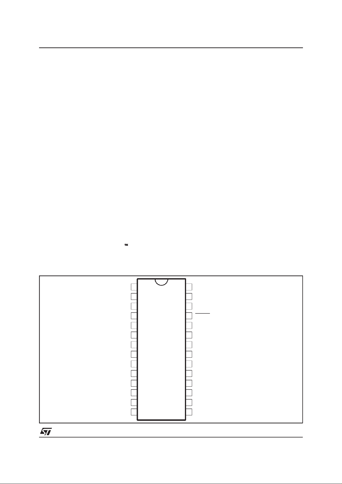
II.1 - Pin Connections
HSYNC
YCRCB7
YCRCB6
YCRCB5
YCRCB4
YCRCB3
YCRCB2
YCRCB1
YCRCB0
V
CVBS
VR_CVBS
I
REF(CVBS)
V
SSA
1
2
3
4
5
6
7
8
9
10
SS
11
12
13
14
28
27
26
25
24
23
22
21
20
19
18
17
16
15
VSYNC/ODDEVEN
SDA
SCL
RESET
CKREF
TTXD
TTXS/CSI2C
V
DD
G/Y
R/C
B/CVBS
VR_RGB
I
REF(RGB)
V
DDA
0119A-01.EPS
3/42

STV0119A
II - PIN INFORMATION (continued)
II.2 - Pin Description
Pin Name Type Function
1 HSYNC I/O Line Synchronization Signal :
2
YCrCb7
3
YCrCb6
4
YCrCb5
5
YCrCb4
6
YCrCb3
7
YCrCb2
8
YCrCb1
9
YCrCb0
10 V
SS
Supply Digital Ground
11 CVBS Output Analog Composite VideoOutput (current-driven).
12 VR_CVBS I/O Internal Reference Voltage forthe 9-bit DAC CVBS.
13 I
REF(CVBS)
14 V
15 V
16 I
REF(RGB)
SSA
DDA
Supply Analog ground for DACs
Supply Analog positive power supply for DACs (+3.3V nom.)
17 VR_RGB I/O Internal reference voltage for the 9bit Tri-DAC R/Y,G/C,B/CVBS.
18 B/CVBS O Analog ‘Blue’ or CVBS output (current-driven).
19 R/C O Analog ‘Red’ orS-VHS Chrominance output (current-driven).
20 G/Y O Analog ‘Green’ or S-VHS Luminance output (current-driven).
21 V
DD
Supply Digital positive supply voltage (+3.3V nom.)
22 TTXS/CSI2C I/O Output : positive sync pulse for control of Teletext buffer in external demultiplexer or
23 TTXD I/O Teletext data stream from external demultiplexer or Transport IC synchronous to rising
- Input in ODDEVEN+HSYNC or VSYNC + HSYNC or VSYNC slave modes
- Output in all other modes (master/slave)
- Synchronous to risingedge of CKREF
- Default polarity : negative pulse
I/O
Input : time multiplexed 4:2:2 luminance and chrominance data as defined in ITU-R
I/O
Rec601-2 and Rec656 (except for TTL input levels).This bus interfaceswith MPEG video
I/O
decoder output port and typically carries a stream of Cb,Y,Cr,Y digital video at CKREF
I/O
frequency, clocked on the rising edge (by default) of CKREF. A 54-Mbit/s ‘double’Cb, Y,
I/O
Cr, Y input multiplex is supported for double encoding application (rising and fallingedge
I/O
of CKREF are operating). Output: for test purpose only.
I/O
I/O
CVBS must be connected to analog ground over a load resistor (R
Following the load resistor, a simple analog low pass filter is recommended CVBS
amplitude is proportional to I
511] V
OUT(Max.)
=1VPPand I
OUT(Max.)
REF(CVBS)(VOUT(N)
= 5mA
=NxR
LOADxIREF(CVBS)
LOAD
).
VR_CVBS must be connected to analog ground over a capacitor (6.8nF typ.),
VR_CVBS = 1.9V
I/O Reference current source for the 9-bit DAC CVBS.
-I
REF(CVBS)
-R
REF(CVBS)(Min.)
(I
REF(CVBS)=VREF(CVBS)/RREF(CVBS)
must be biased to analog ground over a reference resistor R
= 5.95 x R
LOAD/VOUT(Max.)
with V
), V
REF(CVBS)(Typ.)
OUT(Max.)
= 1.12V.
=1VPPand I
OUT(Max.)
REF(CVBS)
I/O Reference current source for Tri-DAC R/Y,G/C,B/CVBS.
-I
REF(RGB)
-R
(I
must be connected to analog ground over a reference resistor R
REF(RGB)(Min.)
REF(RGB)=VREF(RGB)/RREF(RGB)
= 5.95 x R
LOAD/VOUT(Max.)
), V
REF(RGB)(Typ.)
, with V
OUT(Max.)
= 1.12V.
=1VPPand I
OUT(Max.)
VR_RGBmustbe biasedtoanalog ground overa typical 6.8nFcapacitor, VR_RGB = 1.9V.
This output must be connected to analog ground over a load resistor(R
Following the loadresistor, a simple analog low pass filter is recommended.
V
OUT(Max.)
with N = [0-511].
=1VPPand I
OUT(Max.)
= 5mA (V
OUT(N)
=NxR
LOADxIREF(RGB)
This output must be connected to analog ground over a load resistor(R
Following the loadresistor, a simple analog low pass filter is recommended.
V
OUT(Max.)
with N = [0-511].
=1VPPand I
OUT(Max.)
= 5mA (V
OUT(N)
=NxR
LOADxIREF(RGB)
This output must be connected to analog ground over a load resistor(R
Following the loadresistor, a simple analog low pass filter is recommended.
V
OUT(Max.)
with N = [0-511].
=1VPPand I
OUT(Max.)
= 5mA (V
OUT(N)
=NxR
LOADxIREF(RGB)
LOAD
/96)
LOAD
/96)
LOAD
/96)
Transport IC.
edge of CKREF signal averagerate of6.9375Mbit/s.
Output in test mode only.
/96) with N = [0-
= 5mA
REF(RGB)
= 5mA
).
).
).
4/42
II - PIN INFORMATION (continued)
II.2 - Pin Description (continued)
Pin Name Type Function
24 CKREF I Master clock reference signal.
25 RESET I Hardware reset, active LOW.
26 SCL I I
27 SDA I/O I
28 VSYNC/
ODDEVEN
Its rising edge is the default reference for set-up and hold times of all inputs, and for
propagation delay of alloutputs (except for SDA output).
CKREF nominal frequency is 27MHz (CCIR601) : input pad with pull down (50kΩ Typ.)
Ithas priorityoversoftware reset.NRESET imposesdefaultstates(seeRegisterContents).
Minimum Low level required duration is 5 CKREF periods : input pad with pull down
(50kΩ Typ.)
2
C bus clock line (internal 5-bitmajority logic with CKREF forreference) : input pad with
pull down (50kΩTyp.)
2
C bus serial data line.
Input : internal 5-bit majority logic with CKREF for reference
Output : open drain
I/O Frame sync signal :
- input in slave modes, except when sync is extracted from YCrCb data
- output in mastermode and when sync is extracted from YCrCb data
- synchronous to risingedge of CKREF
- ODDEVEN default polarity :
odd (not-top) field :LOW level
even (bottom) field : HIGH level
STV0119A
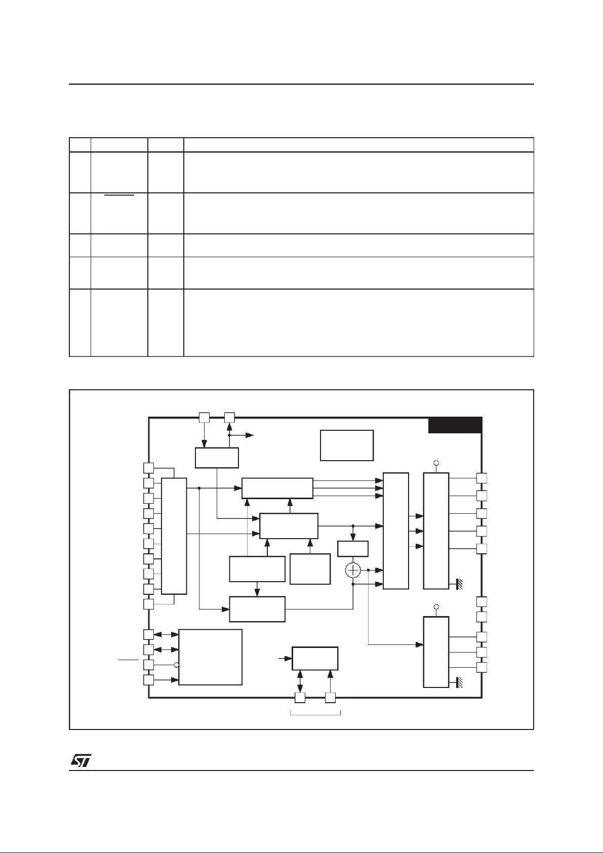
III - BLOCK DIAGRAM
21V
DD
YCRCB7
YCRCB6
YCRCB5
YCRCB4
YCRCB3
YCRCB2
YCRCB1
YCRCB0
VSYNC/ODDEVEN
HSYNC
2
3
4
5
6
7
8
9
10V
SS
28
1
25RESET
24CKREF
TTXS/
CSI2C
TTXD
2223
TELETEXT
CB-CR
Y
DEMULTIPLEXER
SYNC CONTROL
& VIDEOTIMING
GENERATOR
CSI2C
TTXS
RGB ENCODING
PROCESSING
MACROVISION
7.0.1 / 6.1
CHROMA
PROCESSOR
CSI2C
LUMA
CLOSED
CAPTIONS
CGMS
CTRL + CFG
REGISTER
SDA SCL
2
C BUS
I
AUTOTEST
COLORBAR
PATTERN
TRAP
2627
SWITCH
STV0119A
V
DDA
9-BIT TRIDAC
V
DDA
9-BIT
DAC
G/Y
20
R/C
19
B/CVBS
18
VR_RGB
17
I
16
REF(RGB)
V
SSA
V
14
SSA
15
V
DDA
CVBS
11
VR_CVBS
12
I
13
REF(CVBS)
V
SSA
0119A-02.EPS
5/42

STV0119A
IV- FUNCTIONAL DESCRIPTION
TheSTV0119Acanoperateeither inmastermode,
where it supplies all sync signals, or in 6 slave
modes,whereit locksonto incoming sync signals.
The main functions are controlledby a micro-controller via an I
Register Description” for an exhaustive list of the
controlpossibilitiesavailable.
IV.1 - Data Input Format
The digital input is a time-multiplexed ITU-R656
/D1-type [Cb, Y, Cr, Y] 8-bit stream. Note that
”ITU-R” wasformerlyknownas”CCIR”.Inputsamples are latched in on the rising edge (by default)
of the clock signal CKREF, whose nominal frequencyis 27MHz.Figure1 illustratesthe expected
datainputformat.Alternatively,a 54-Mbit/sstream
canbe fed to the STV0119A,referto SectionIV.17
(”dualencoding”) for details.
The STV0119Ais able to encode interlaced and
non-interlacedvideo. One bit is sufficient to automatically direct the STV0119Ato process non-interlaced video. Update is performed internally on
the first frame sync active edge followingthe programing of this bit. The non-interlaced mode is a
624/2= 312 line mode or a 524/2= 262 line mode,
whereall fieldsare identical.
An ‘autotest’ mode is available by setting 3 bits
(sync[2:0]) within the configurations register0.
Inthis mode, a color barpatternis produced,independentlyfrom video input, in the adequatestandard. As this mode sets the STV0119A in master
mode, VSYNC/ODDEVEN and HSYNC pins are
thenin outputmode.
IV.2 - VideoTiming
The STV0119A outputs interlaced or non-interlacedvideo in PAL-B,D, G, H, I,PAL-N,PAL-Mor
NTSC-Mstandards and ‘NTSC- 4.43’is also possible.
The4-frame (for PAL)or 2 frame(for NTSC)burst
sequences are internally generated, subcarrier
generation being performed numerically with
CKREF as reference. Rise and fall times of synchronizationtips andburstenveloppeareinternally
controlled according to the relevant ITU-R and
SMPTErecommendations.
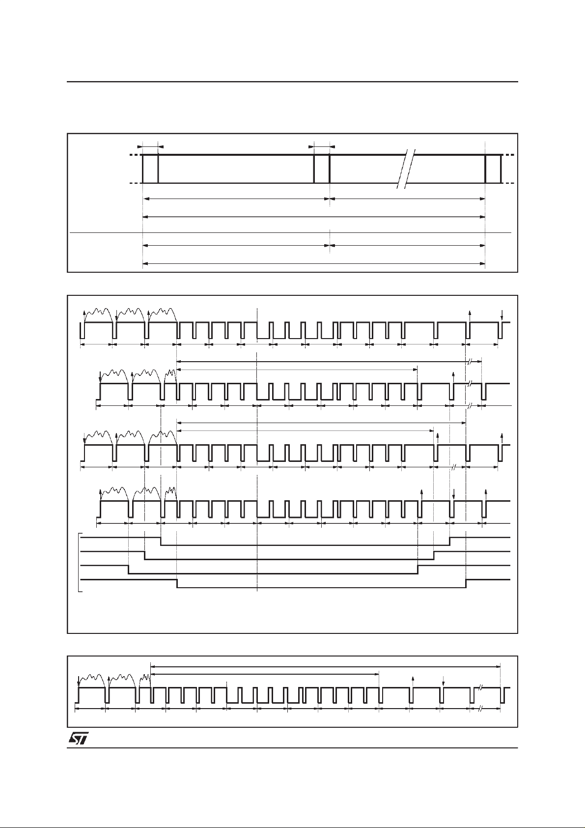
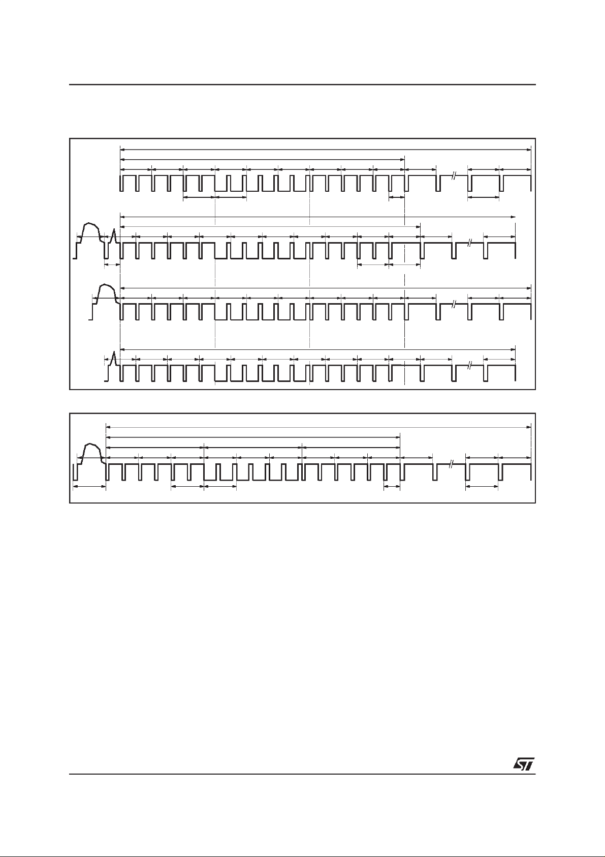
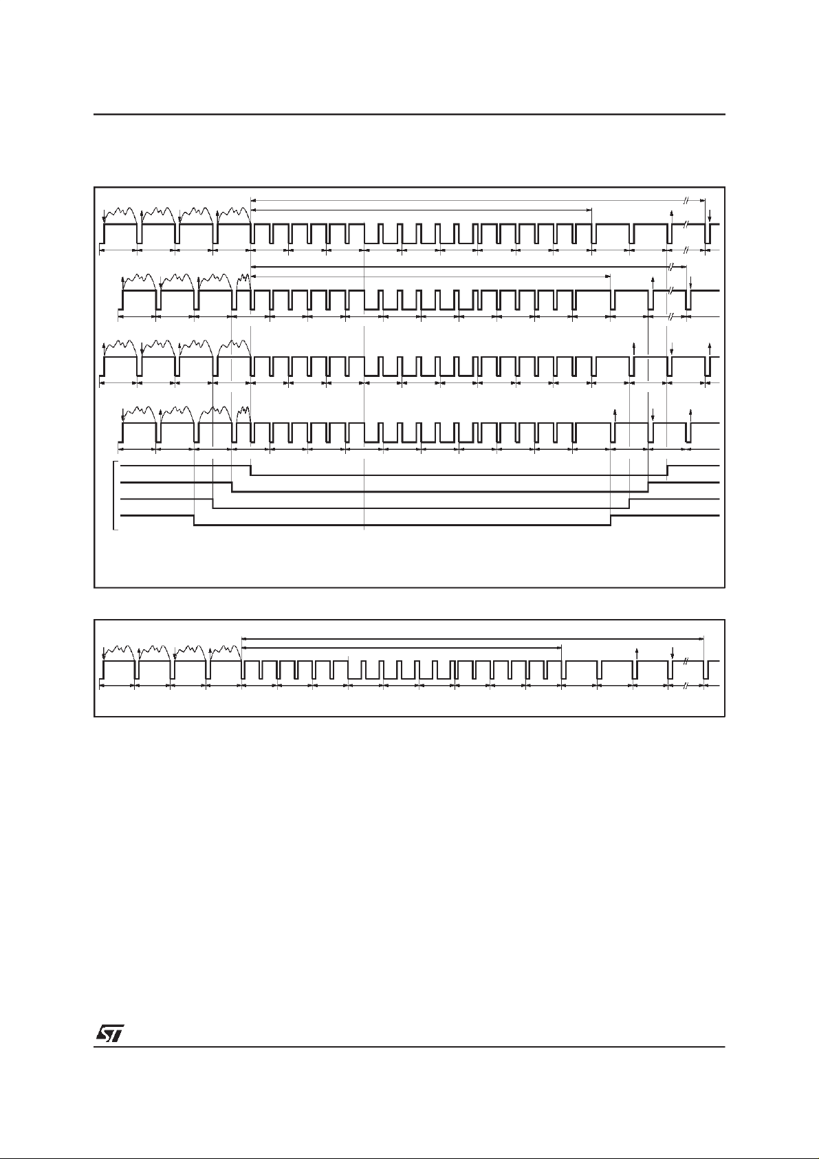
Figures2 to 7 depicttypicalVBI waveforms.
It is possible to allow encodingof incomingYCrCb
dataon those lines of the VBIthat do not bearline
sync pulses or pre/post-equalisation pulses (see
Figures2 to 7). This mode of operationis refered
to as ”partial blanking”and is the default set-up. It
2
C 2-wire bus. Refer to the ”User’s
allows to keep in the encoded waveform any VBI
data present in digitized form in the incoming
YCrCb stream (e.g. WSS data, VPS, supplementary Closed-Captions line or StarSight data, etc.).
Alternatively,thecompleteVBImaybe blanked(no
incomingYCrCbdata encodedon theselines, ”full
blanking”).
ThecompleteVBI comprisesof the followinglines:
- for 525/60systems(SMPTEline numberingconvention): lines1 to19 andsecond half ofline 263
to line 282.
- for 625/50 systems (CCIR line numbering convention) : second half of line 623 to line 22 and
lines 311to 335.
The ‘partial’VBI consists of :
- for 525/60systems(SMPTEline numberingconvention): lines1 to 9 andsecond halfof line263
to line 272.
- for 625/50 systems (CCIR line numbering convention):secondhalf of line623toline 5andlines
311to 318.
Fullorpartialblankingis controlledby configuration
bit ‘blkli in configurationregister1’.
Note that :
- line 282 in 525/60/SMPTEsystemsis either fully
blankedor fullyactive.
- line 23 in 625/60/CCIR systems is always fully
active.
InanITU-R656-compliantdigitalTVline, theactive
portion of the digital line is the portion included
between the SAV (Start of Active Video) and EAV
(End of Active Video) words. However, this digital
active line starts somewhat earlier and may end
slightlylater than the active line usually definedby
analog standards. The STV0119A allows two approaches:
- It is possible to encode the full digital line (720
pixels/ 1440clockcycles).Inthiscase,theoutput
waveform will reflect the full YCrCb stream included between SAVand EAV.
- Alternatively,it is possible to drop some YCrCb
samples at the extremities of the digital line so
that the encoded analog line fits within the ‘analog’ ITU-R/SMPTEspecifications.
Selection between these two modes of operation
is performed with bit ‘aline’in configurationregister 4.
In all cases, the transitions between horizontal
blankingand activevideo areshaped to avoid too
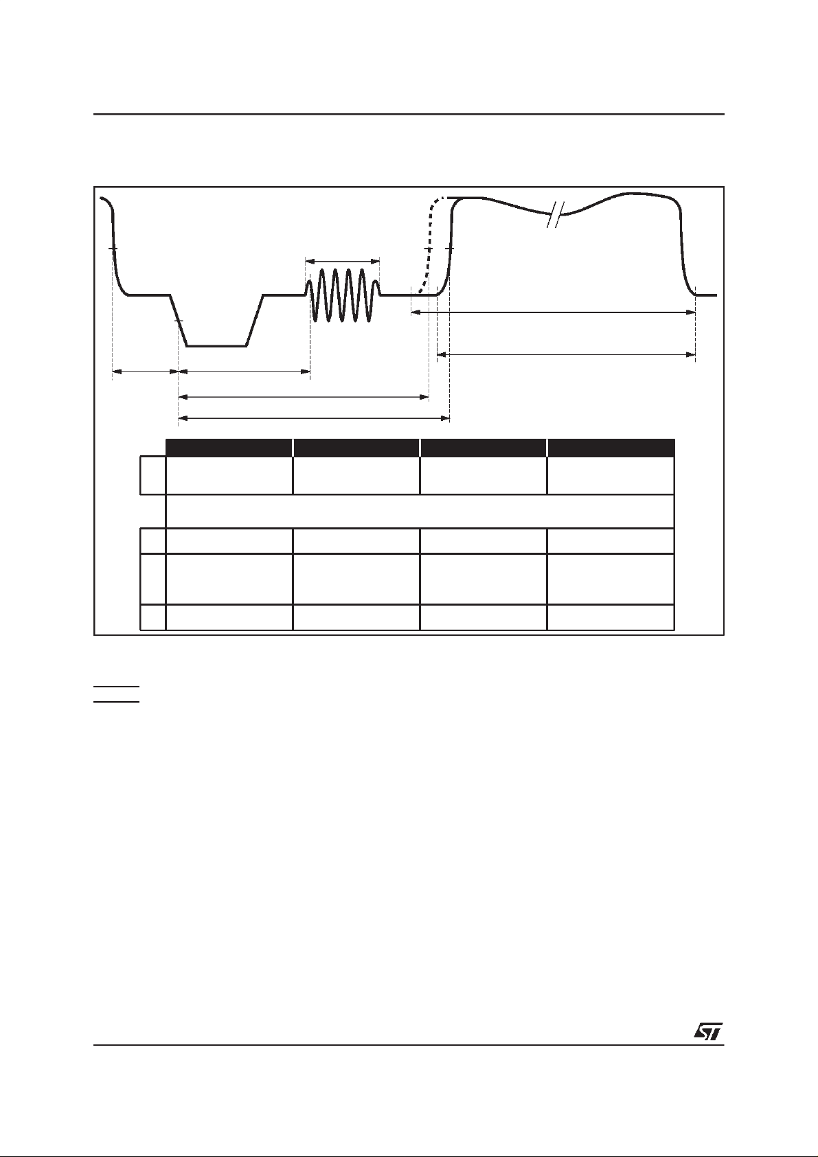
steepedgeswithin theactive video.Figure 8 gives
timingsconcerning the horizontalblankinginterval
and the active video interval.
6/42
IV- FUNCTIONAL DESCRIPTION(continued)
Figure1 : InputData Format
STV0119A
4T4T
E
A
V
276T
Digital Standing Interval
(525 Line / 60Hz)
S
A
V
1716T
1440T
Digital Active LineNTSC, PAL M
Line Duration
PAL B, D, G, H, I, N
(625 Line / 50Hz)
288T
1728T
1440T
Figure2 : PAL-BDGHI,PAL-N TypicalVBI Waveform,InterlacedMode (CCIR-625 Line Numbering)
0
V
IV
308 309 310 311 312 313 314 315 316 317 318 319 320
PartialVBI1
624 625 1 2 3 4 5 6 7 23621 622 623
Partial VBI2
Full VBI1
I
Full VBI2
A
II
AB
A
22
E
A
V
0119A-08.EPS
335
C
:
0
V
I, II, III, IV :
A:
B:
C:
311 312 313 314 315 316 317 318 317 336308 309 310
62462512345678621 622 623
Frame synchronizationreference
st
1
and 5th,2ndand6th,3rdand 7th,4thand 8thfields
Burst phase : nominal value +135°
Burst phase : nominal value -135°
Burst suppressioninternal
III
AB
I
II
III
IV
Figure3 : PAL-BDGHI,PAL-NTypicalVBI Waveform,Non-interlaced Mode (“CCIR-like” LineNumbering)
Full VBI
AB
22
7/42
Burst phase toggles every line
0
V
31131212345678308 309 310
PartialVBI
0119A-09.EPS
0119A-10.EPS
STV0119A
IV- FUNCTIONAL DESCRIPTION(continued)
Figure4 : NTSC-MTypical VBI Waveforms,InterlacedMode (SMPTE-525Line Numbering)
1
23
Partial VBI1
45678910 1819
Full VBI1
Partial VBI2
Full VBI2
HH0.5H
VBI3
12345678910 1819525
VBI4
H0.5HHH
282273272271270269268267266265264263262
282273272271270269268267266265264263
Figure5 : NTSC-MTypical VBI Waveforms,Non-interlacedMode (“SMPTE-like” Line Numbering)
Full VBI
PartialVBI
262
1
H
233H4563H7893H10 18 19
H0.5HHH
0119A-11.EPS
0119A-12.EPS
8/42
IV- FUNCTIONAL DESCRIPTION(continued)
Figure6 : PAL-MTypical VBI Waveforms,InterlacedMode (CCIR-525 Line Numbering)
F’
0
PartialVBI1
V
I
FullVBI1
STV0119A
AB
519F520F’521F522 523 524 525 1 2 3 4 5 6 7 8 9
F
257F’258F259 260
F
519F’520F521 522
F’
257F258 259 260
C
0V:
Framesynchronizationreference
I, II, III, IV :
1stand5th,2ndand6th,3rdand7th,4thand8thfields
A:
Burstphase: nominalvalue +135°
B:
Burstphase: nominalvalue -135°
C:
Burstsuppressioninternal
261 262 263 264 265 266 267 268 269 270 271 280
523 524 525 1 2 3 4 5 6 7 8 9
261 262 263 264 265 266 267 268 269 270 271 272
PartialVBI2
II
III
IV
I
II
III
IV
FullVBI2
AB
AB
Figure7 : PAL-MTypical VBI Waveforms,Non-interlacedMode(“CCIR-like” Line Numbering)
0
V
Partial VBI
Full VBI
AB
16 17
AB
279
0119A-13.EPS
256257258259260261262123456789
Burstphase toggles every line
10 16 17
0119A-14.EPS
9/42
STV0119A
IV- FUNCTIONAL DESCRIPTION(continued)
Figure8 : Horizontal Blanking Intervaland Active VideoTimings
d
0
H
b
a
(bit”aline” = 0)
c1
c2 (bit ”aline” =1)
Full Digital Line Encoding
(720Pixels - 1440T)
”Analog” Line Encoding
(710Pixels - 1420T)
NTSC-M
5.38µs(even lines)
a
5.52µs(odd lines)
Actual values will depend on the static offset programmed for subcarrier generation.
b
c1
c2
d
1.56µs
8.8µs
9.3µs
9 Cycles of 3.58MHz
PAL-BDGHI
5.54µs(A-type)
5.66µs(B-type)
Theseare typical values.
1.28µs
9.3µs
10.1µs
10 Cyclesof 4.43MHz
IV.3 - Reset Procedure
Ahardwareresetis performedbygroundingthe Pin
RESET. Themasterclockmustberunningand Pin
RESET kept low for a minimum of 5 clockcycles.
This sets the STV0119A in HSYNC+ODDEVEN
(line-locked) slave mode, for NTSC-M, interlaced
ITU-R601encoding with Macrovision
TM
copyprotection revision 7.01 operating. Closed-captioning
and Teletextencodingare all disabled.
Then the configuration can be customizedby writing into the appropriate registers. A few registers
PAL-N
5.54µs(A-type)
5.66µs(B-type)
1.28µs
9.3µs
10.1µs
9 Cycles of 3.58MHz
PAL-M
5.73µs(A-type)
5.87µs(B-type)
1.28µs
9.3µs
10.1µs
9 Cycles of 3.58MHz
are never reset,their contentsis unknownuntilthe
first loading (refer to the Register Contents and
Description).
It is also possible to perform a software reset by
settingbit’softreset’in Reg6. The IC’sresponsein
that caseis similarto itsresponseaftera hardware
reset, except that Configuration Registers
(Reg0 to6) anda few otherregisters(seedescription of bit‘softreset’)are not altered.
0119A-15.EPS
10/42
STV0119A
IV- FUNCTIONAL DESCRIPTION(continued)
IV.4 - MasterMode
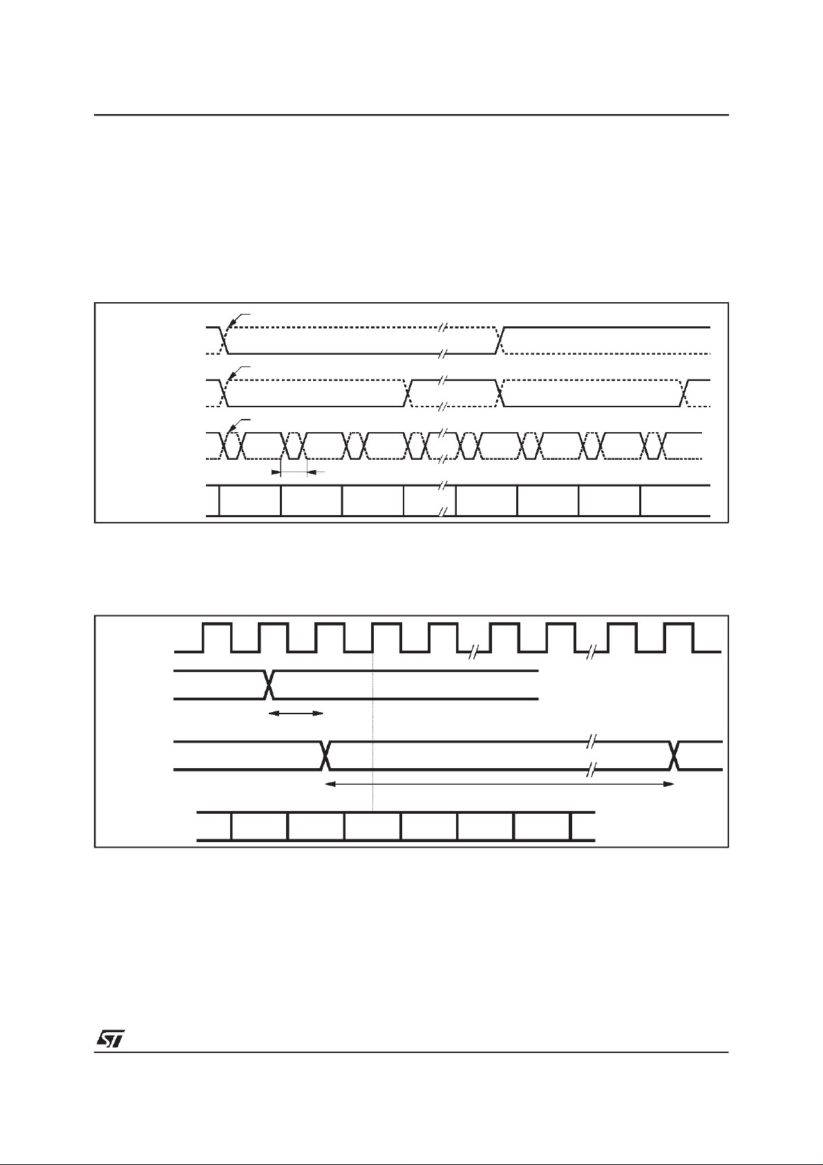
In this mode, the STV0119Asupplies HSYNC and
ODDEVEN sync signals (with independentlyprogrammablepolarities) to drive other blocks. Refer
to Figure9 and 10 for timings and waveforms.
TheSTV0119Astartsencodingand countingclock
Figure9 : ODDEVEN,VSYNC and HSYNC Waveforms
Active edge (programmable polarity)
ODDEVEN
(see Note 1)
Active edge (programmable polarity)
VSYNC
Active edge (programmable polarity)
HSYNC
(see Note 2)
Line Numbers :
SMPTE-525
CCIR-62541
Notes : 1. When ODDEVEN is a sync input, only one edge (“the active edge”) of the incoming ODDEVEN is taken into account for
synchronization. The “non-active” edge (2nd edge on thisdrawing) is not critical andits position may differ by H/2 from the location
shown.
2. The HSYNC pulse width indicated is valid when the STV0119Asupplies HSYNC.In those slave modes where it receives HSYNC,
only the edge defined as activeis relevant,and thewidthof the HSYNC pulse it receives is not critical.
128 T
5
2
6
3
ckref
= 4.74µs
cycles as soon as the master mode has been
loadedinto thecontrol register(Reg.0).
Configuration bits ”Syncout_ad[1:0]”(Reg4) allow
toshiftthe relativepositionofthesyncsignalsbyup
to 3 clockcyclesto copewith anyYCrCb phasing.
266
313
267
314
268
315
269
316
0119A-16.EPS
Figure10 : MasterMode Sync Signals
CKREF
ODDEVEN
(out)
HSYNC
(out)
YCRCB
Note : 1. This figureis valid for bits “syncout_ad[1:0]” = default.
Active Edge
(programmable polarity)
1T
CKREF
Cr Y’
Active Edge
(programmable polarity)
Cb Y Cr Y’
Duration of HSYNC Pulse : 128T
CKREF
0119A-17.EPS
11/42
STV0119A
IV- FUNCTIONAL DESCRIPTION(continued)
IV.5 - SlaveModes
Sixslavemodesareavailable:ODDEVEN+HSYNC
based (line-based sync), VSYNC+HSYNC based
(anothertype of line-basedsync),ODDEVEN-only
based(frame-basedsync),VSYNC-onlybased(another type of frame-based sync), or sync-in-data
based(line lockedor framelocked).
ODDEVEN refers to an odd/even (also known as
not-top/bottom) field flag, HSYNC is a line sync
signal,VSYNCis a verticalsyncsignal.Theirwaveforms are depicted in Figure 9. The polarities of
HSYNC and VSYNC/ODDEVEN a re independentlyprogrammablein all slave modes.
IV.5.1- Synchronizationontoa LineSyncSignal
IV.5.1.1- HSYNC+ODDEVENBased
Synchronization
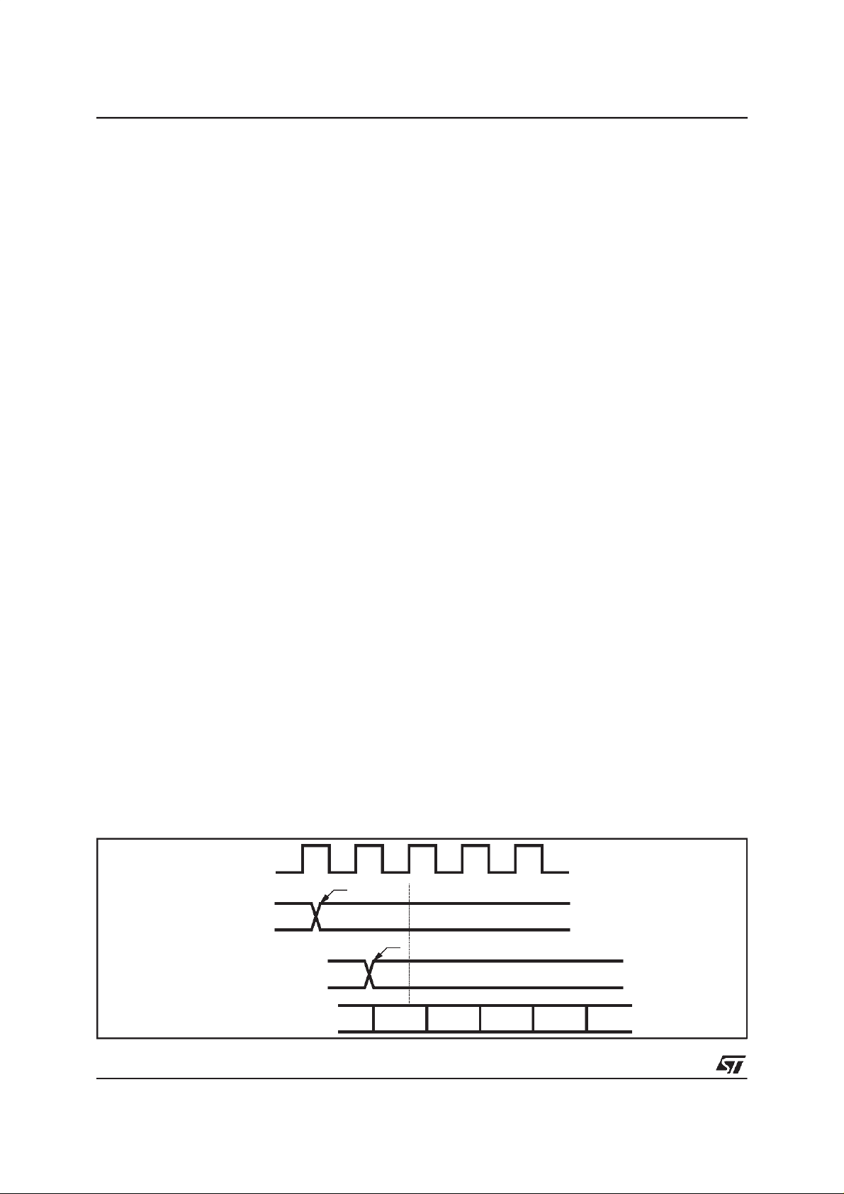
Synchronizationis performedon a line-by-line basis by locking onto incoming ODDEVEN and
HSYNCsignals. Refer to Figure 11for waveforms
and timings. The polarities of the active edges of
HSYNC and ODDEVEN are programmable and
independent.
The first active edge of ODDEVEN initializes the
internal line counter but encoding of the first line
does not start until an HSYNC active edge is detected(at theearliest,HSYNCmaytransitionat the
sametimeas ODDEENV).Atthatpoint,the internal
sample counter is initialized and encoding of the
firstlinestarts.Then,encodingof eachsubsequent
line is individually triggered by HSYNC active
edges. The phase relationship between HSYNC
andthe incomingYCrCB data isnormallysuchthat
the first clock rising edge following the HSYNC
active edge samples ”Cb” (i.e. a ‘blue’ chroma
sample within the YCrCb stream). It is however
possibleto internallydelay the incoming sync signals (HSYNC+ODDEVEN) by up to 3 clockcycles
to cope with different data/sync phasings, using
Figure11 : HSYNC+ ODDEVENBased Slave Mode Sync Signals
configurationbits ”Syncin_ad”(Reg. 4).
The STV0119Ais thus fully slaved to the HSYNC
signal, which means that lines may contain more
or less samples than typical 525/625 system requirement.
If the digital line is shorter than its nominal value:
the samplecounterisre-initializedwhenthe ‘early’
HSYNC arrives and all internal synchronization
signals are re-initialized.
If the digital line is longer than its nominal value :
the sample counter is stoppedwhen it reachesits
nominal end-of-line value and waits for the ‘late’
HSYNCbefore reinitializing.
ThefieldcounterisincrementedoneachODDEVEN
transition. The line counteris reset on the HSYNC
followingeachactiveedgeof ODDEVEN.
IV.5.1.2- HSYNC + VSYNC Based Synchronization
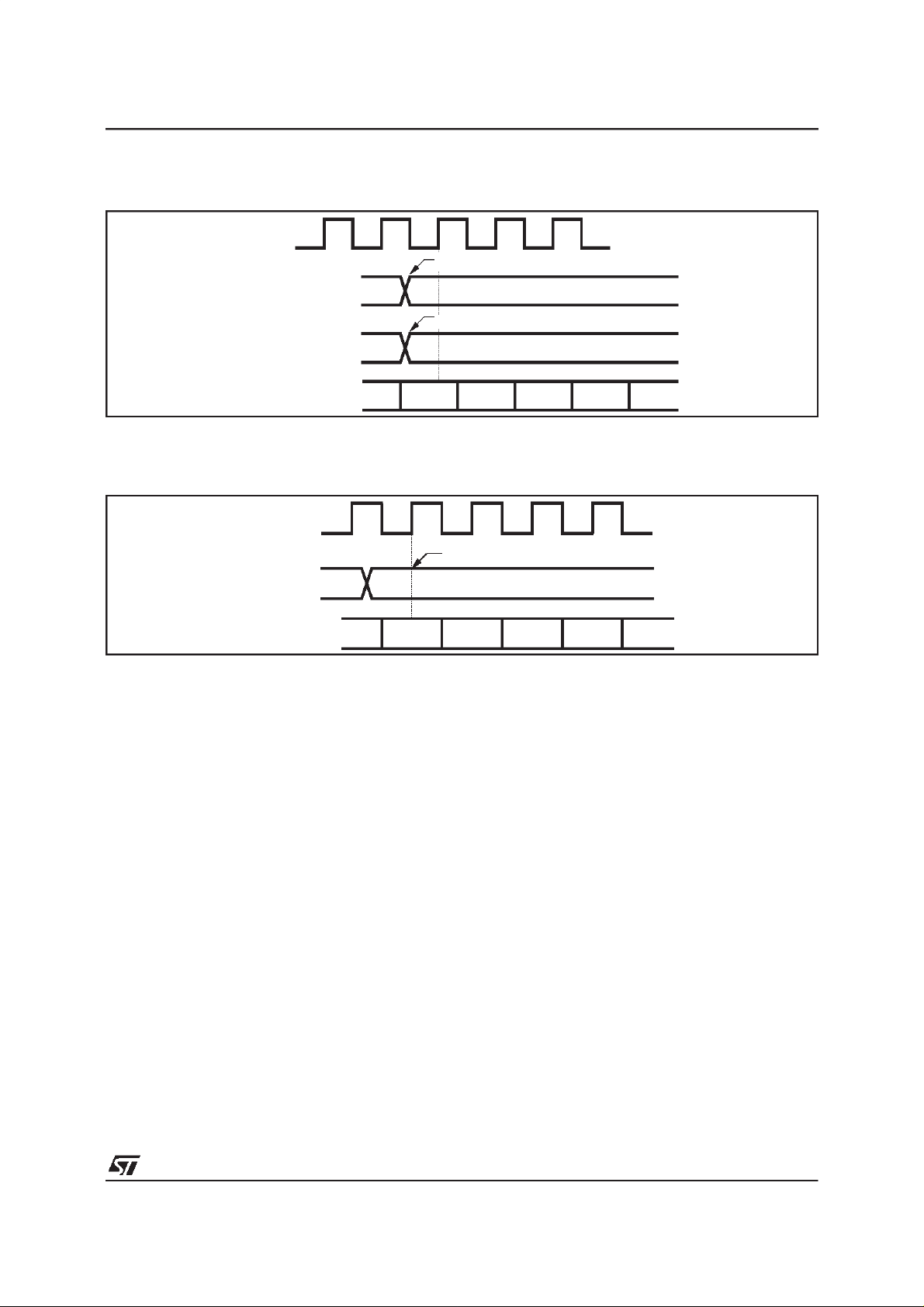
Synchronizationis performed on a line-by-linebasis by locking onto incoming VSYNC and HSYNC
signals. Refer to Figure 12 for waveforms and
timings. The polaritiesof HSYNC and VSYNC are
programmableand independent.
The incomingVSYNC signal is immediately transformed into a waveform identical to the odd/even
waveform of an ODDEVEN signal, therefore the
behavior of the core is identical to that described
aboveforODDEVEN+HSYNCbased synchronization. Again, the p hase relationship between
HSYNC and the incoming YCrCb data is normally
such that the first clock rising edge following the
HSYNC active edge samples ”Cb” (i.e. a ‘blue’
chroma sample within the YCrCb stream). It is
however possible to internally delay the incoming
sync signals (HSYNC+VSYNC) by up to 3 clock
cycles to cope with different data/sync phasings,
using configurationbits ”Syncin_ad” (Reg.4).
The field counter is incremented on each active
edge of VSYNC.
CKREF
ActiveEdge (programmablepolarity)
ODDEVEN
(in)
HSYNC
(in)
YCRCB
Note : 1. This figure is valid for bits “syncin_ad[1:0]” = default.
12/42
ActiveEdge (programmablepolarity)
Cb Y Cr Y’ Cb
0119A-18.EPS
IV- FUNCTIONAL DESCRIPTION(continued)
Figure12 : HSYNC+ VSYNC Based Slave Mode Sync Signals
CKREF
Active Edge (programmablepolarity)
VSYNC
(in)
Active Edge (programmablepolarity)
HSYNC
(in)
STV0119A
YCRCB Cb Y Cr Y’ Cb
Notes : 1. This figure is valid for bits “syncin_ad[1:0]” = default.
2. The active edges of HSYNC and VSYNC should normally be simultaneous. It is permissible that HSYNC transitions before
VSYNC, but VSYNC must not transition before HSYNC.
Figure13 : ODDEVENBased Slave Mode Sync Signals
CKREF
Active Edge (programmable polarity)
ODDEVEN
(in)
YCRCB
Note : 1. This figure is valid for bits “syncin_ad[1:0]” = default.
IV .5 .2-Synchro niza t ionontoa FrameSyncSignal
IV .5.2.1- ODDEVEN- onl yBasedSynchronizati on
Synchronizationis performedona frame-by-frame
basisby lockingonto an incoming ODDEVEN signal. A line sync signal is derived internally and is
also output as HSYNC. Refer to Figure 13 for
waveforms and timings. The phase relationship
betweenODDEVENand the incomingYCrCB data
is normally such that the first clock rising edge
followingthe ODDEVENactiveedge samples”Cb”
(i.e. a ‘blue’ chroma sample within the YCrCb
stream). It is however possible to internally delay
the incoming ODDEVEN signal by up to 3 clock
cycles to cope with different data/sync phasings,
using configurationbits ”Syncin_ad”(Reg. 4).
Thefirstactiveedgeof ODDEVENtriggersgenerationofthe analogsyncsignalsand encodingof the
incomingvideo data.Framesbeingsupposedtobe
of constant duration, the next ODDEVEN active
transitionisexpectedat aprecisetimeafterthelast
ODDEVENdetected.
So, once an active ODDEVEN edge has been
detected,checks that the followingODDEVENare
presentat the expected instantsare performed.
Encodingandanalog sync generationcarry on un-
Cb Y Cr Y’ Cb
less three successive fails of these checks occur.
In that case,three behaviorsare possible,accord-
ing to the configurationprogrammed(Reg. 1-2) :
- if ‘free-run’is enabled, the STV0119A carries on
outputtingthe digitalline syncHSYNCand generating analog video just as though the expected
ODDEVEN edge had been present. However, it
willre-synchronizeontothenextODDEVENactive
edgedetected,whateverits location.
- if ‘free-run’ is disabled but bit ‘sync_ok’ is set in
configuration register1, the STV0119A sets the
active portion of the TV line to black level but
carrieson outputtingthe analog sync tips (on Ys
and CVBS) and the digital line sync signal
HSYNC. (When programmed, Macrovision
pseudo-sync pulses and AGC pulses are also
presentin the analog syncwaveform).
- if ‘free-run’is disabledand the bit‘sync_ok’is not
set, allanalog video is at blacklevel and neither
analog sync tips nor digital line sync are output.
Note that this mode is a frame-basedsync mode,
asopposedtoa field-basedsyncmode,thatis,only
one type of edge (rising or falling,according to bit
‘polv’in Reg 0) is of interest to the STV0119A,the
other one is ignored.
0119A-19.EPS
0119A-20.EPS
TM
13/42
 Loading...