

SGS Thomson Microelectronics STV0056AF Datasheet
SATELLITESOUNDAND VIDEO PROCESSOR
SOUND
.
TWO INDEPENDENT SOUND DEMODULATORS
.
PLL DEMODULATION WITH 5-10MHz FREQUENCYSYNTHESIS
.
PROGRAMMABLE FM DEMODULATOR
BANDWIDTH ACCOMODATING FM DEVIATIONSFROM ±30kHz TILL ±400kHz
.
PROGRAMMABLE 50/75µs, J17 OR NO DEEMPHASIS
.
WEGENERPANDASYSTEM
.
TWO AUXILIARYAUDIOINPUTS AND OUTPUTS
.
GAIN CONTROLLED AND MUTEABLE
AUDIOOUTPUTS
.
HIGH IMPEDANCE MODE AUDIO OUTPUTS
FORTWINTUNERAPPLICATIONS
VIDEO
.
COMPOSITE VIDEO 6-bit 0 to 12.7dB GAIN
CONTROL
.
COMPOSITEVIDEOSELECTABLEINVERTER
.
TWO SELECTABLE VIDEO DE-EMPHASIS
NETWORKS
.
6 x 3 VIDEOMATRIX
.
BLACK LEVEL ADJUSTABLE OUTPUT FOR
ON-BOARDVIDEOCRYPTDECODER
.
HIGH IMPEDANCE MODE VIDEO OUTPUTS
FORTWINTUNERAPPLICATIONS
MISCELLANEOUS
.
22kHzTONEGENERA TI ONFORLNBCONTROL
.
I2C BUSCONTROL
CHIPADDRESSES= 06
.
LOW POWER STAND-BY MODE WITH ACTIVEAUDIOANDVIDEO MATRIXES
HEX
OR46
HEX
STV0056AF
TQFP64 (10 x 10mm)
(Thin Plastic Quad Flat Pack)
ORDER CODE : STV0056AF
DESCRIPTION
TheSTV0056AFBICMOSintegratedcircuit realizes
allthenecessarysignalprocessingfromthetunerto
theAudio/Videoinputandoutputconnectorsregardlessthe satellitesystem.
February 1998
1/27
STV0056AF
PIN CONNECTIONS
GND
S2 VID OUT
VOL L
S2 VID RTN
S2 OUTL
CLAMP IN
S2 OUTR
UNCL DEEM
VIDEEM2/22kHz
V 12V
V 12V
VIDEEM1
VGND
VGND
NC
B-BAND IN
S2 RTN L
S2 RTNR
FM IN
S3 RTN L
S3 RTNR
AGC L
S3 OUT L
S3 OUTR
SCL
SDA
HA
J17 R
J17 L
XTL
V
DD
1213141516
17
18
19
20
21
22
23
24
25
IO
26
27
28
29
30
31
32
5V
38 39 40 41 42 43 44 45 46 47 4833 34 35 36 37
NC
GND 5V
U75 L
DET L
CPUMP L
NC
AGC R
AMPLKL
REF
V
A 12V
AGND L
AGND L
A 12V
1234567891011
DET R
AMPLK R
PIN ASSIGNMENT
Pin Number Name Function
1 GND Connected to the Lead Frame
2 S2 VID OUT VCR-Scart 2 VideoOutput
3 VOL L Volume Controlled Audio Out Left
4 S2 VID RTN VCR-Scart 2 Video Return
5 S2 OUT L Fixed Level Audio OutputLeft (to VCR)
6 CLAMP IN Sync-Tip Clamp Input
7 S2 OUT R Fixed Level Audio OutputRight (to VCR)
8 UNCL DEEM Unclamped Deemphasized Video Output
9 VIDEEM2/22kHz Video Deemphasis 2 or 22kHz Output
10 - 11 V 12V Video 12V Supply
12 VIDEEM1 Video Deemphasis 1
13 - 14 V GND Video Ground
15 NC
16 B-BAND IN Base Band Input
17 S2 RTN L Auxiliary Audio Return Left (from VCR)
18 S2 RTN R Auxiliary Audio Return Right (from VCR)
19 FM IN FM Demodulator Input
20 S3 RTN L Auxiliary Audio Return Left (from decoder)
64
S1 VIDOUT
63
S3 VIDOUT
62
VOL R
61
S3 VIDRTN
60
S1 VIDRTN
59
LEVELR
58
PKIN R
57
FCR
56
AGNDR
55
FCL
54
PKIN L
53
LEVELL
52
PKOUTL
51
PKOUTR
50
I
49
U75 R
REF
CPUMPR
0056F-01.EPS
0056F-01.TBL
2/27

PIN ASSIGNMENT(continued)
Pin Number Name Function
21 S3 RTN R Auxiliary Audio Return Right (from decoder)
22 AGC L AGC Peak Detector Capacitor Left
23 S3 OUT L Auxiliary Audio Output L (to decoder)
24 S3 OUT R Auxiliary Audio Output R (to decoder)
25 I/O/22kHz Digital Input/Output or 22kHz Output
26 SCL I
27 SDA I
28 HA Hardware Address
29 J17 R J17 Deemphasis Time Constant Right
30 J17 L J17 Deemphasis Time Constant Left
31 XTL 4/8MHz Quartz Crystal or Clock Input
32 V
5V Digital 5V Power Supply
DD
34 NC Not Connected
33 GND 5V Digital Power Ground
35 CPUMP L FM PLL Charge Pump Capacitor Left
36 DET L FM PLL Filter Left
37 U75 L Deemphasis Time Constant Left
38 AMPLK L Amplitude Detector Capacitor Left
39 AGC R AGC Peak Detector Capacitor Right
40 NC
41 - 42 A GND L Audio Ground
43 V
REF
44 - 45 A 12V Audio 12V Supply
46 AMPLK R Amplitude Detector Capacitor Left
47 DET R FM PLL Filter Right
48 U75 R Deemphasis Time Constant Right
49 CPUMP R FM PLL Charge Pump Capacitor Right
50 I
REF
51 PK OUT R Noise Reduction Peak Detector Output Right
52 PK OUT L Noise Reduction Peak Detector Output Left
53 LEVEL L Noise Reduction Level Left
54 PK IN L Noise Reduction Peak Detector Input
55 FC L Audio Roll-off Left
56 A GND R Audio Ground
57 FC R Audio Roll-off Right
58 PK IN R Noise Reduction Peak Detector Input Right
59 LEVEL R Noise Reduction Level Right
60 S1 VID RTN TV-Scart 1 Video Return
61 S3 VID RTN Decoder-Scart Video Return
62 VOL R Volume Controlled Audio Out Right
63 S3 VID OUT Decoder-Scart Video Output
64 S1 VID OUT TV-Scart 1 VideoOutput
2
C Bus Clock
2
C Bus Data
2.4V Reference
Current Reference Resistor
STV0056AF
0056F-01.TBL
3/27

STV0056AF
PIN DESCRIPTION
1 - Sound Detection
FMIN
This is the input to the two FM demodulators. It
feeds two AGC amplifiers with a bandwidth of at
least 5-10MHz. There is one amplifier for each
channelboth withthe sameinput. TheAGC amplifiers have a 0dB to +40dBrange.
=5kΩ, Mininput = 2mVPPper subcarrier.
Z
IN
Max input = 500mV
addedtogether,when their phases coincide).
AGC L, AGC R
AGC amplifiers peak detector capacitor connections.The output current hasan attack/decayratio
of 1:32. That is the ramp up current is approximately 5µA and decay current is approximately
160µA. 11V gives maximum gain. These pins are
also driven by a circuit monitoring the voltage on
AMPLKL and AMPLK R respectively.
AMPLKL, AMPLK R
The outputs of amplitude detectors LEFT and
RIGHT.Eachrequiresa capacitorand a resistorto
GND. The voltage across this is used to decide
whetherthereis a signalbeing receivedby the FM
detector.The level detector output drives a bit in
the detectorI
2
C bus controlblock.
AMPLK L and AMPLK R drive also respectively
AGCLand AGCR. For instancewhen the voltage
on AMPLK L is > (V
frompin AGCLto reduce the AGCgain.
V
REF
DET L, DETR
Respectivelythe outputsofthe FMphasedetector
leftand right.
This is for the connectionof an external loop filter
for the PLL. The output is a push-pull current
source.
CPUMPL, CPUMPR
The output from the frequency synthesizer is a
push-pullcurrentsourcewhichrequiresa capacitor
(max when all inputs are
PP
+1VBE) it sinks current to
REF
to groundto derivea voltageto pull the VCOto the
target frequency.The outputis ±100µA to achieve
lockand±2µAduringlocktoprovidea trackingtime
constant of approximately10Hz.
V
REF
This isthe audio processorvoltage referenceused
through out the FM/audio section of the chip. As
such it is essential that it is well decoupled to
ground to reduce as far as possible the risk of
crosstalk and noise injection. This voltage is derived directlyfrom the bandgapreferenceof 2.4V.
The V
output can sink up to 500µA in normal
REF
operationand 100µAwhen in stand-by.
I
REF
Thisis abufferedV
outputtoan off-chipresistor
REF
to produce an accurate current reference, within
the chip, for the biasing of amplifiers with current
outputs into filters.It is also required for the Noise
reduction circuit to provide accurate roll-off frequencies. This pin should not be decoupled as it
would inject current noise. The target current is
50µA±2% thusa 47.5kΩ ±1% is required.
A 12V
Double bonded main power pin for the audio/FM
section of the chip. The two bond connectionsare
to the ESD and to power the circuit and on chip
regulators/references.
A GND L
This groundpin is double bonded :
1) to channelLEFT : RF section & VCO,
2) to both AGC amplifiers, channel LEFT and
RIGHTaudio filtersection.
A GND R
This groundpin is double bonded :
1) to the volume control, noise reduction system,
ESD + Mux + V
REF
2) to channelright : RF section& VCO
4/27

PIN DESCRIPTION(continued)
2 - Baseband Audio Processing
PK OUT L, PK OUT R, PK OUT
The noise reduction control loop peak detector
outputrequiresa capacitortogroundfrom thispin,
and a resistor to V
pin to give some accurate
REF
decaytimeconstant.Anonchip5kΩ ±25%resistor
and external capacitor give the attack time.
PK IN L, PK IN R or PK IN
Eachof thesepinsis an inputtoa controllooppeak
detector and is connected to the output of the
offchipcontrolloop band pass filter.
STV0056AF
U75 L, U75 R
External deemphasis networks for channels left
andright.Foreachchannelacapacitorandresistor
in parallel of 75µs time constant are connected
betweenhereandV
sis. Internallyselectableis an internalresistor that
canbeprogrammedto beaddedin parallelthereby
convertingthe network to approx 50µs de-emphasis (see controlblock map). The value of theinternal resistors is 54kΩ ±30 %. The amplifier for this
filter is voltage input, current output ; with ±500mV
input the output will be ±55µA.
toprovide75µsde-empha-
REF
LEVELL, LEVELR
Respectivelythe audio left and right signals of the
FMdemodulators are output to level L and level R
pins through an input follower buffer. The off-chip
filters driven by these pins must include AC couplingto thenext stage (PK IN L and PK IN R pins
respectively).
FC L, FC R
The variable bandwidth transconductance amplifier has a currentoutput which is variabledependingon the input signalamplitude as defined by the
control loop of the noise reduction. The output
current is then dumped into an off-chip capacitor
whichtogetherwith the accuratecurrent reference
definethemin/maxrolloff frequencies.Aresistorin
serieswith acapacitoris connectedtoground from
thesetwo pins.
J17 L, J17 R
The external J17 de-emphasisnetworks for channels left and right. The amplifier for this filter is
voltageinput, current output. Output with ±500mV
input will be ±55µA.
ToperformJ17 de-emphasiswiththeSTV0042,an
externalcircuit isrequired.
VOLL, VOL R
The main audio output from the volume control
amplifierthe signalto get output signalsas highas
2V
(+12dB) on a DC bias of 4.8V. Control is
RMS
from +12dB to -26.75dB plus Mute with 1.25dB
steps.Thisamplifierhasshortcircuitprotectionand
is intendedto drivea SCARTconnectordirectlyvia
AC couplingand meetsthe standardSCART drive
requirements. These outputs feature high impedance mode forparallel connection.
S2 OUT L, S2 OUT R, S3 OUT L, S3 OUT R
These audio outputs are sourced directly from the
audio MUX, and as a result do not include any
volume control function. They will output a 1V
RMS
signal biased at 4.8V.They are short circuit protected. These outputs feature high impedance
mode for parallel connection and meet SCART
drive requirement.
S2 RTN L, S2 RTN R, S3 RTN L, S3 RTN R
These pins allow auxiliaryaudio signalsto be connected to the audio processor and hence makes
use of the on-chip volume control. For additional
detailsplease refer to the audio switchingtable.
5/27

STV0056AF
PIN DESCRIPTION(continued)
3 - Video Processing
B-BAND IN
AC-coupledvideo input from a tuner.
Z
> 10kΩ ±25%. This drives an on-chip video
IN
amplifier. The other input of this amp is AC
groundedby being connectedto an internalV
The video amplifier has selectable gain from 0dB
to 12.7dB in 63 steps and its output signal can be
selectednormalor inverted.
UNCLDEEM
Deemphasizedstill unclamped output.It isalso an
input of the video matrix.
VIDEEM1
Connected to an external de-emphasis network
(forinstance 625 lines PALde-emphasis).
VIDEEM2/ 22kHz
Connected to an external de-emphasis network
(forinstance525linesNTSCorothervideo de-emphasis).Alternativelyaprecise22kHz tonemaybe
output by I
2
C bus control.
CLAMPIN
This pin clamps the most negative extreme of the
input(the sync tips)to 2.7V
(or appropriatevolt-
DC
age). The video at the clamp input is only 1V
This clamped video which is de-emphasised, filtered and clamped (energy dispersal removed) is
normal, negative syncs, video. This signal drives
the Video Matrixinput called Normal Video.
It hasa weak(1.0µA ±15 %) stablecurrentsource
pullingthe inputtowardsGND. Otherwisethe input
impedanceis very high at DC to 1kHz Z
Video bandwidth through this is -1dB at 5.5MHz.
TheCLAMP input DC restore voltageis then used
as a means for getting the correct DC voltage on
the SCART outputs.
S3 VID RTN
This input can be driven for instance by the decoder.This input hasa DC restorationclampon its
input.Theclampsink current is 1µA ±15%with the
bufferZ
>1MΩ.
IN
S2 VID RTN, S1 VID RTN
Externalvideoinput1.0VppACcoupled75Ωsource
impedance.This input has a DC restorationclamp
on its input. The clamp sink current is 1µA ±15%
withthe bufferZ
>1MΩ.This signalis an input to
IN
the Video Matrix.
>2MΩ.
IN
REF
PP
onthe O/P. Thesignalis video2.0V
PP
with sync tip = 1.2V.These pins get signals from
the Video Matrix. The signal selected from the
Video Matrix for output on this pin is controlled by
a control register. This output also feature a high
impedancemode for parallel connection.
.
S3 VID OUT
This output can drive for instance a decoder. Also
it is able to pass 10MHz ; Z
this pin will be 2V
. The black level of the ouput
PP
<75Ω. Video on
OUT
video signal can be adjusted through I
trol to easily interface with on-board Videocrypt
decoder. This output feature an high impedance
mode for parallel connection.
V 12V
+12Vdoublebonded: ESD+guardringsandvideo
circuitpower.
V GND
Doubledbonded.Clean VID INGND. Strategically
placed video power ground connection to reduce
video currents getting into the rest of the circuit.
4 - ControlBlock
GND 5V
.
The main power ground connectionfor the control
logic, registers, the I
2
C bus interface, synthesizer
& watchdogand XTLOSC.
VDD5V
Digital +5V power supply.
SCL
Thisis theI2C busclockline.Clock=DCto100kHz.
Requiresexternal pull up eg. 10kΩ to 5V.
SDA
This isthe I2Cbus data line.Requiresexternalpull
up eg. 10kΩ to 5V.
I/O / 22kHz
Generalpurposeinput outputpin or 22kHz output.
XTL
Thispinallowsfor theon-chiposcillatorto beeither
used with a crystal to ground of 4MHzor 8MHz,or
to be driven by an external clock source. The
external source can be either 4MHz or 8MHz. A
programmablebitinthecontrol blockremovesa ÷2
block when the 4MHz option is selected.
5.5MHzBW
2
C bus con-
S1 VID OUT,S2 VID OUT
Video drivers for SCART 1 and SCART 2. An
externalemitter follower buffer is requiredto drive
a 150Ω load. The average DC voltage to be 1.5V
6/27
HA
Hardwareaddresswith internal 135µApull down.
Chip address is 06 when this pin is grouded and
chip address is 46 when connectedto V
DD
.
GENERAL BLOCKDIAGRAM
STV0056AF
From Tuner
Video
Processing
FromTV,
VCR/Decoder
FM
B-BAND
From Tuner
Demodulation
2 Channels
Wegener
Panda+
Deemphasis
22kHz to LNB
STV0056AF
VIDEOPROCESSINGBLOCK DIAGRAM
LPF
I/O/22kHz
B-BAND IN
25
22kHz
TONE
16
± 1
G
2
2
6x3
Video
4
Matrix
Audio
Matrix
+
Volume
2
I
C Bus
Interface
NTSC
PAL
VIDEEM1VIDEEM2/22kHz
9128
Baseband
3
3
To TV, VCR/Decoder
Active in Stand-by
UNCLDEEM
Deemphasized
÷ 2
0056F-02.EPS
CLAMPIN
S3 VID RTN
S2 VID RTN
S1 VID RTN
6
CLAMP
CLAMP
61
CLAMP
4
CLAMP
60
STV0056AF
Normal
DecoderReturn
VCRReturn
TV Return
BLACKLEVEL
ADJUST
63
64 2
To Decoder To VCR
S1 VID OUT
S2 VID OUTS3 VID OUT
To TV
0056F-03.EPS
7/27
STV0056AF
AUDIO PROCESSINGBLOCK DIAGRAM (CHANNELRIGHT)
AUDIO R
47
a
ANRS
K3
b
4
abc
K4
b
a
K6
-6dB -6dB
24 21 51 58 59 57 7 18 62
AUDIO
DEEMPHASIS
29 48
STV0056AF
K2
a
ba
c
abc
6dB6dB
K1
b
c
K5
MONO
STEREO
DET R
PLL
FILTER
Audio
Decoder Out
FC R
PK IN R
S3 OUT R
S3 RTN R
Audio
Decoder Return
LEVEL R
PK OUT R
J17 R
U75 R
DECODER VCR
AUDIO PROCESSINGBLOCK DIAGRAM(CHANNELLEFT)
AUDIOL
36
a
ANRS
K3
K4
abc
K6
23 20 52 54 53 55 5 17 3
b
a
-6dB -6dB
b
4
AUDIO
DEEMPHASIS
30 37
S2 OUT R
S2 RTN R
STV0056AF
K2
a
ba
c
abc
6dB6dB
K1
b
c
K5
MONO
STEREO
VOL R
TV
0056F-04.EPS
8/27
DET L
PLL
FILTER
Decoder Out
FC L
PK IN L
S3 OUT L
Audio
S3 RTN L
Audio
DecoderReturn
DECODER VCR
LEVEL L
PK OUT L
J17 L
U75 L
S2 OUT L
S2 RTN L
VOL L
TV
0056F-05.EPS
AUDIO SWITCHING
STV0056AF
AUDIO
DEEMPHASIS
+ ANRS
AUDIOPLL
DECRTN
AUXIN K
K
1a
K
1b
1c 6b
VOL OUT AUXOUT
K
K
K
5b
5c
5a
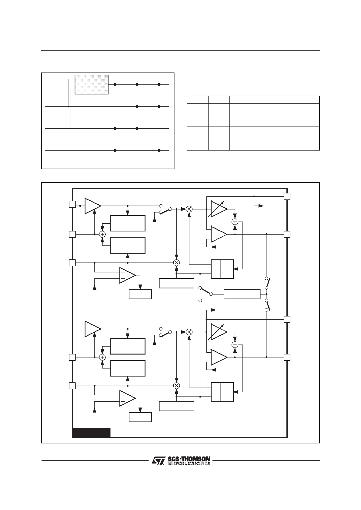
FM DEMODULATION BLOCK DIAGRAM
FM IN
19
AGC
LEVEL
DETECTOR1
AGC R
39
LEVEL
DETECTOR2
K
K
K
DECOUT
Bias
6c
6a
SW1
0056F-06.EPS
Phase
Detect
:a→ANRS input non-scrambledaudio
K
4
b → ANRS input descrambledaudio
K
a
b
b
c
a
b
b
c
K
2
1
2
1
2
3
a
No ANRS, No De-emphasis
a
No ANRS, 50µs
a
No ANRS, 75µs
a
No ANRS, J17
b
ANRS, No De-emphasis
b
ANRS, 50µs
b
ANRS, 75µs
b
ANRS, J17
AUDIOR
FM dev.
Select.
V
REF
47
49
DET R
CPUMPR
AMPLKR
AGC L
AMPLK L
46
V
REF
AGC
22
38
V
REF
STV0056AF
Reg8 b4
LEVEL
DETECTOR1
LEVEL
DETECTOR2
Reg8 b0
Amp.Detect
WATCHDOG
SW3
Bias
Amp.Detect
WATCHDOG
Phase
Detect
90
VCO
0
SYNTHESIZER
AUDIOL
FM dev.
Select.
V
REF
90
VCO
0
SW2
SW4
36
35
DET L
CPUMP L
0056F-07.EPS
9/27
 Loading...