

SGS Thomson Microelectronics STV0042A Datasheet
SATELLITESOUNDAND VIDEO PROCESSORS
SOUND
.
TWO INDEPENDENTSOUNDDEMODULATORS
.
PLL DEMODULATION WITH 5-10MHz
FREQUENCY SYNTHESIS
.
PROGRAMMABLE FM DEMODULATOR
BANDWIDTH ACCOMODATING FM DEVIATIONSFROM±30kHz TILL±400kHz
.
PROGRAMMABLE 50/75µs OR NO DE-EMPHASIS
.
DYNAMICNOISEREDUCTION
.
ONE OR TWO AUXILIARY AUDIO INPUTS
ANDOUTPUTS
.
GAIN CONTROLLED AND MUTEABLE
AUDIOOUTPUTS
.
HIGH IMPEDANCE MODE AUDIO OUTPUTS
FORTWINTUNER APPLICATIONS
VIDEO
.
COMPOSITE VIDEO 6-bit 0 to 12.7dB GAIN
CONTROL
.
COMPOSITE VIDEO SELECTABLE INVERTER
.
TWO SELECTABLE VIDEO DE-EMPHASIS
NETWORKS
.
4 x 2 VIDEOMATRIX
.
HIGH IMPEDANCE MODE VIDEO OUTPUTS
FORTWINTUNER APPLICATIONS
MISCELLANEOUS
.
22kHzTONEGENERA TI ONFORLNBCONTROL
.
I2C BUS CONTROL :
CHIPADDRESSES= 06
.
LOW POW ER STAND-BYMODEWITH ACTIVE
AUDIO ANDVIDEOMATRIXES
DESCRIPTION
TheSTV0042ABICMOSintegratedcircuitrealizes
all the necessarysignal processingfrom the tuner
to the Audio/Video input and output connectors
regardlessthe satellite system.
The STV0042 is intended for low cost satellite
receiverapplication.
HEX
(Plastic Package)
ORDER CODE : STV0042A
PIN CONNECTIONS
FC R
PK IN
SUM OUT
VOL R
S1 VID OUT
S2 VID OUT
VOL L
S2 VID RTN
S2 OUT L
CLAMP IN
S2 OUT R
UNCL DEEM
VIDEEM2/22kHz
V 12V
VIDEEM1
V GND
B-BANDIN
S2 RTN L
S2 RTN R
FM IN
STV0042A
PRODUCT PREVIEW
SHRINK42
1
2
3
4
5
6
7
8
9
10
11
12
13
14
15
16
17
18
19
20
21 22
A GND R
42
FC L
41
PK OUT
40
I
39
REF
CPUMP R
38
U75 R
37
DET R
36
AMPLK R
35
A 12VA 12V
34
V
33
32
31
30
29
28
27
26
25
24
23
REF
A GND L
AGC R
AMPLK L
U75 L
DET L
CPUMP L
GND 5V
5V
V
DD
XTL
SDA
SCLAGC L
0042A-01.EPS
March 1997
1/24

STV0042A
PIN ASSIGNMENT
Pin Number Name Function
1 FC R Audio Roll-off Right
3 SUM OUT Noise Reduction Summing Output
2 PK IN Noise Reduction Peak Detector Input
4 VOL R Volume Controlled Audio Out Right
5 S1 VID OUT TV-Scart 1 Video Output
6 S2 VID OUT VCR-Scart 2 Video Output
7 VOL L Volume Controlled Audio Out Left
8 S2 VID RTN VCR-Scart2 VideoReturn
9 S2 OUT L Fixed Level Audio Output Left
10 CLAMP IN Sync-Tip Clamp Input
11 S2 OUTR Fixed Level Audio Output Right
12 UNCL DEEM Unclamped Deemphasized Video Output
13 VIDEEM2/22kHz Video Deemphasis 2 or 22kHz Output
14 V 12V Video 12V Supply
15 VIDEEM1 Video Deemphasis 1
16 V GND Video Ground
17 B-BAND IN Base Band Input
18 S2 RTN L Auxiliary Audio Return Left
19 S2 RTN R Auxiliary Audio Return Right
20 FM IN FM Demodulator Input
21 AGC L AGC Peak Detector Capacitor Left
22 SCL I
23 SDA I
24 XTL 4/8MHz QuartzCrystal or Clock Input
25 V
5V Digital 5V Power Supply
DD
26 GND 5V Digital Power Ground
27 CPUMP L FM PLL Charge Pump Capacitor Left
28 DET L FM PLL Filter Left
29 U75 L Deemphasis Time Constant Left
30 AMPLK L Amplitude Detector Capacitor Left
31 AGC R AGC Peak Detector Capacitor Right
32 A GND L Audio Ground
33 V
REF
34 A 12V Audio 12V Supply
35 AMPLK R Amplitude Detector Capacitor Left
36 DET R FM PLL Filter Right
37 U75 R Deemphasis Time Constant Right
38 CPUMP R FM PLL Charge Pump CapacitorRight
39 I
REF
40 PK OUT Noise Reduction Peak Detector Output
41 FC L Audio Roll-off Left
42 A GND R Audio Ground
2
C Bus Clock
2
C Bus Data
2.4V Reference
Current Reference Resistor
0042A-01.TBL
2/24

PIN DESCRIPTION
1 - Sound Detection
FMIN
This is the input to the two FM demodulators. It
feeds two AGC amplifiers with a bandwidth of at
least 5-10MHz. There is one amplifier for each
channelboth with the sameinput.TheAGCamplifiers have a 0dB to +40dBrange.
=5kΩ, Min input =2mVPPper subcarrier.
Z
IN
Max input = 500mV
(max when all inputs are
PP
addedtogether,when their phases coincide).
AGC L, AGC R
AGC amplifiers peak detector capacitor connections.The outputcurrent has an attack/decayratio
of 1:32. That is the ramp up current is approximately 5µA and decay current is approximately
160µA. 11V gives maximumgain. These pins are
also driven by a circuit monitoring the voltage on
AMPLKL andAMPLK R respectively.
AMPLKL, AMPLK R
The outputs of amplitude detectors LEFT and
RIGHT.Eachrequiresa capacitorand a resistorto
GND. The voltage across this is used to decide
whetherthereis a signalbeing receivedby the FM
detector.The level detector output drives a bit in
the detectorI
2
C bus control block.
AMPLK L and AMPLK R drive also respectively
AGCL and AGC R. For instance when thevoltage
on AMPLK L is > (V
V
frompin AGCLto reduce the AGCgain.
REF
+1VBE) it sinks current to
REF
DET L, DETR
Respectivelythe outputsof the FMphasedetector
left and right. This is for the connection of an
external loop filter for the PLL. The output is a
push-pullcurrent source.
CPUMPL, CPUMPR
The output from the frequency synthesizer is a
push-pullcurrentsourcewhichrequiresa capacitor
togroundto derivea voltageto pullthe VCOto the
targetfrequency.The output is ±100µAto achieve
lockand ±2µAduringlocktoprovidea trackingtime
constantof approximately10Hz.
VREF
Thisisthe audio processorvoltagereferenceused
through out the FM/audio section of the chip. As
such it is essential that it is well decoupled to
ground to reduce as far as possible the risk of
crosstalk and noise injection. This voltage is derived directly from the bandgapreference of 2.4V.
The V
output can sink up to 500µA in normal
REF
operationand 100µAwhen in stand-by.
IREF
Thisis abufferedV
outputto an off-chipresistor
REF
to produce an accurate current reference, within
STV0042A
the chip, for the biasing of amplifierswith current
outputs into filters.It is also required for the Noise
reduction circuit to provide accurate roll-off frequencies.
This pin should not be decoupled asit would inject
currentnoise.The targetcurrentis 50µA±2%thus
a 47.5kΩ ±1% is required.
A 12V
Double bonded main power pin for the audio/FM
section of the chip. The two bond connectionsare
to the ESD and to power the circuit and on chip
regulators/references.
A GND L
This ground pin is double bonded :
1) to channel LEFT : RF section & VCO,
2) to both AGC amplifiers, channel LEFT and
RIGHTaudio filter section.
A GND R
This ground pin is double bonded :
1) to the volume control, noise reduction system,
ESD + Mux + V
2) to channel right : RF section& VCO
2 - BasebandAudioProcessing
PK OUT
The noise reduction control loop peak detector
outputrequiresa capacitorto groundfrom this pin,
and a resistor to V
decaytimeconstant.Anon chip5k
and externalcapacitor give the attack time.
PK IN
This pin is an inputto a controlloop peak detector
andis connectedto theoutputof the offchipcontrol
loop bandpass filter.
SUM OUT
The two audio demodulated signals are summed
togetherbymeansofanamplifierwithagainof0.5.
If both inputs are 1V then the output is 1V. This
amplifierhas an input followerbufferwhich givesa
offset in the DC bias voltage. Thus the filter
V
BE
which this amplifier drives must include AC coupling to the next stage (PK IN Pin).
FC L, FC R
The variable bandwidth transconductance amplifier has a currentoutput which is variabledepending on the input signalamplitude as definedby the
control loop of the noise reduction. The output
current is then dumped into an off-chip capacitor
whichtogetherwith the accurate current reference
definethe min/maxrolloff frequencies.Aresistorin
serieswitha capacitorisconnectedto ground from
these two pins.
REF
pin to give some accurate
REF
Ω ±
25%resistor
3/24

STV0042A
PIN DESCRIPTION(continued)
U75 L, U75 R
Exter naldeemphasi snetwor k s for channels left and
right. For each channel a capaci t or and resistor in
parallelof 75µ stimeconstantare connect edbetween
hereandV
select abl e is an internal resis tor that can be programmedtobeaddedinparal lelthere byconvertingthe
netwo r ktoapprox50µsde-emphasis(seecontro lblock
map ).Thevalueoftheinter nalresistorsis30k Ω ±30%.
Theampli fi erforthisfilterisvoltageinput,currentoutput;
with ±500m Vinputtheoutputwil lbe±55 µ A.
VOLL, VOL R
Themainaudiooutputfromthevol umecontrolamplifier
the signal to get output signals as high as 2V
(+12dB)ona DCbiasof4.8V.Controlisfrom+12dBto
-26.7 5dBplus Mute with 1.25dBsteps.Thisamplifi er
has short circuit protection and is intended to drive a
SCARTconnectordirectlyvia AC coupli n gandmeets
thestandar dSCARTdri v erequi rements.Thes eoutpu ts
featur ehighimped ancemodeforparallelconnection.
S2 OUT L, S2 OUT R
These audio outputs are sourced directl y from the
audioMUX,andas aresultdonotincludeanyvolume
controlfunction.Theywilloutputa1V
at4.8V .Theyareshortcircui tprotected.Theseoutputs
featurehigh impedancemodefor parallelconnectio n
andmeetSCARTdriverequirement.
S2 RTN L, S2 RTN R
Thesepins allowauxiliary audiosignals to be connected to the audio processor and hence makes
use of the on-chip volume control. For additional
detailsplease refer to the audio switching table.
3 - VideoProcessing
B-BAND IN
AC-coupledvideo input from a tuner.
Z
>10k
IN
fier.TheotherinputofthisampisACgroundedbybeing
connectedtoaninterna lV
selectablegainfrom0dBto12.7dBin63stepsandits
outputsignalcanbe selectednormalorinverted.
UNCLDEEM
Deemphasizedstill unclamped output.It isalso an
input of thevideo matrix.
VIDEEM1
Connected to an external de-emphasis network
(forinstance 625 lines PALde-emphasis).
VIDEEM2/ 22kHz
Connected to an external de-emphasis network
(forinstance525lines NTSCor othervideode-emphasis).Alternativelyaprecise22kHztone maybe
output by I
CLAMPIN
Thispinclampsthemostnegativeextremeoftheinput
(thesynctips) to2.7V
4/24
toprov i d e75µsde-emph as i s.Internally
REF
signalbiased
RMS
Ω ±
25%.Thisdrivesanon-chipvideoampli-
.Thevideoamplifierhas
REF
2
C bus control.
(orappropriat evoltage) .The
DC
RMS
video at the clamp input is only 1V
.Thisclamped
PP
video which is de-e mph as i s ed,filter ed and clamped
(energydispersa lremoved)isnormal,negativesyncs,
video.Thissignaldrivesthe VideoMatrixinputcalled
Normal Video. It has a weak (1.0µA ±15 %) stable
currentsourcepullingtheinput toward sGND .Otherwise theinput impedanceis veryhigh atDC to 1kHz
>2MΩ. Video bandwidth through this is -1dB at
Z
IN
5.5MHz.TheCLAMPinputDCrestorevoltageis then
usedasameansforgettingthecorrectDCvoltageon
theSCARToutputs.
S2 VID RTN
External video input 1.0VPPAC coupled 75
Ω
sourceimpedance.This input hasa DCrestoration
clamp on its input. The clamp sink current is 1µA
±
15% withthe bufferZ
>1MΩ. Thissignal is an
IN
input to the VideoMatrix.
S1 VID OUT,S2 VID OUT
VideodriversforSCART1andSCART2.Anexternal
emitterfollowerbufferisrequiredto drivea 150 Ωload.
TheaverageDC voltageto be 1.5V on the O/P.The
signalisvideo2.0V
5.5MHzBWwithsynctip=1.2V.
PP
These pins get signals from the Video Matrix. The
signalselectedfromtheVideoMatri xforoutputon this
piniscontrolledbya controlregister.Thisoutputalso
featureahighimpedancemodeforparallelconnection.
V 12V
+12Vdoublebonded : ESD+guardringsand video
circuitpower.
V GND
Doubledbonded.Clean VID INGND. Strategically
placed video power ground connection to reduce
video currents getting into the rest of the circuit.
4 - Control Block
GND 5V
The main power ground connectionfor the control
logic, registers, the I
2
C bus interface, synthesizer
& watchdog and XTLOSC.
VDD 5V
Digital +5V powersupply.
SCL
Thisis theI2C busclockline.Clock= DCto100kHz.
Requiresexternal pull up eg. 10kΩto 5V.
SDA
This is the I2Cbus dataline. Requires externalpull
up eg. 10kΩ to5V.
XTL
Thispinallowsfor theon-chiposcillatorto beeither
used with a crystaltoground of 4MHzor 8MHz, or
to be driven by an external clock source. The
external source can be either 4MHz or 8MHz. A
programmablebitinthecontrolblockremovesa÷2
block when the 4MHzoption is selected.
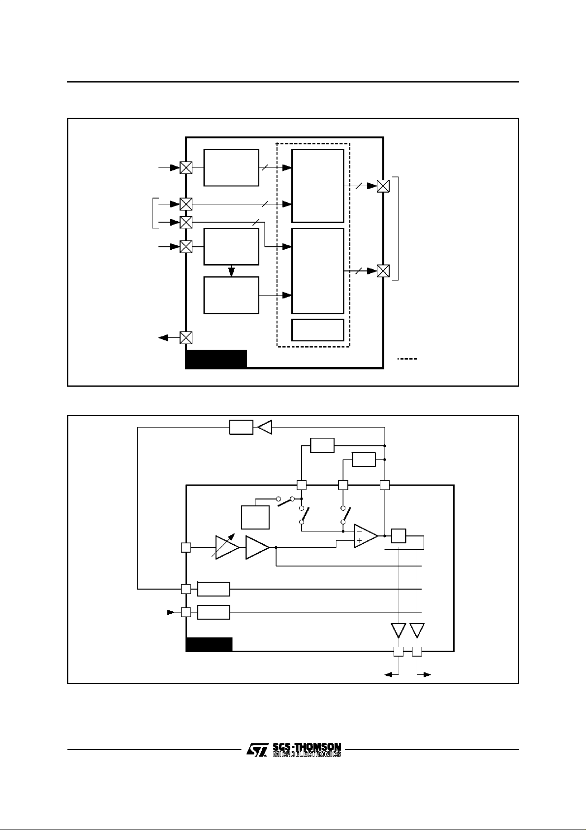
GENERAL BLOCK DIAGRAM
STV0042A
From Tuner
Video
Processing
From
VCR/Decoder
FM
B-BAND
From Tuner
Demodulation
2 Channels
Noise
Reduction+
Deemphasis
22kHzto LNB
STV0042A
VIDEOPROCESSINGBLOCK DIAGRAM
LPF
2
4x2
Video
2
Matrix
2
1
To TV, VCR/Decoder
Audio
Matrix
2
+
Volume
2
I
C Bus
Interface
Active in Stand-by
0042A-02.EPS
B-BAND IN
CLAMP IN
S2 VID RTN
17
CLAMP
10
CLAMP
8
STV0042A
NTSC
PAL
VIDEEM1VIDEEM2/22kHz
13 15 12
22kHz
TONE
± 1
G
Baseband
Normal
VCR / Decoder Return
To Decoder or VCR To TV
UNCL DEEM
Deemphasized
÷ 2
56
S1 VID OUTS2 VID OUT
0042A-03.EPS
5/24
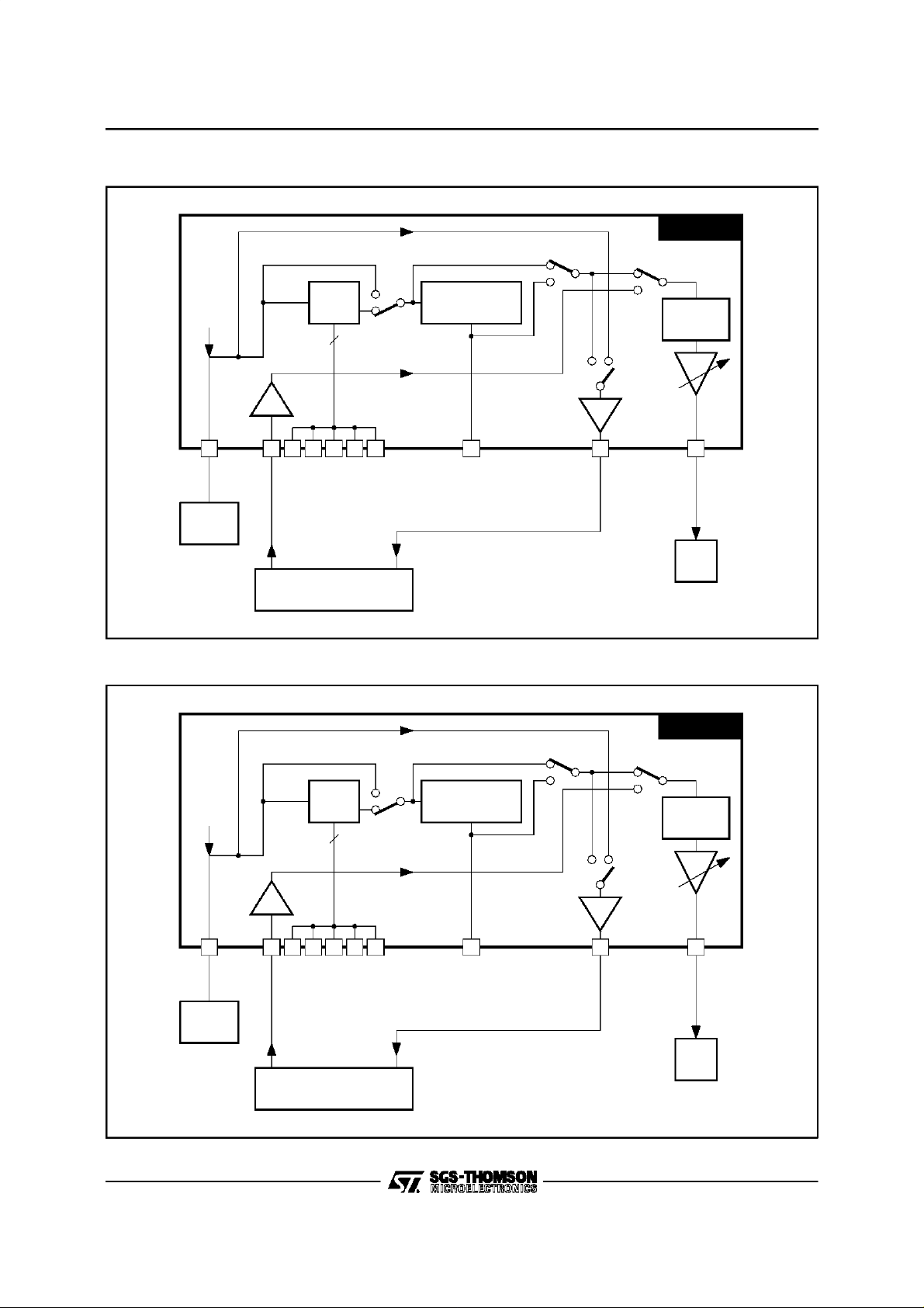
STV0042A
AUDIO PROCESSINGBLOCK DIAGRAM(CHANNEL RIGHT)
STV0042A
K2a
K1a
PK IN
5
SUM OUT
a
K3
b
FC L
FC R
ANRS
AUDIO R
-6dB
36 19 40 2 3 1 41 37 11 4
DET R
PLL
FILTER
PK OUT
S2 RTN R
DECODER OR VCR
AUDIO
DEEMPHASIS
U75 R
AUDIO PROCESSINGBLOCK DIAGRAM(CHANNELLEFT)
b
c
MONO
STEREO
bc
K5
6dB
VOL R
S2 OUT R
TV
0042A-04.EPS
STV0042A
K2a
K1a
6/24
b
c
bc
K5
6dB
S2 OUT L
PK IN
5
SUM OUT
a
K3
b
FC L
FC R
ANRS
AUDIO L
-6dB
28 18 40 2 3 1 41 29 9 7
DET L
PLL
FILTER
PK OUT
S2 RTN L
DECODER OR VCR
AUDIO
DEEMPHASIS
U75 L
MONO
STEREO
VOL L
TV
0042A-05.EPS
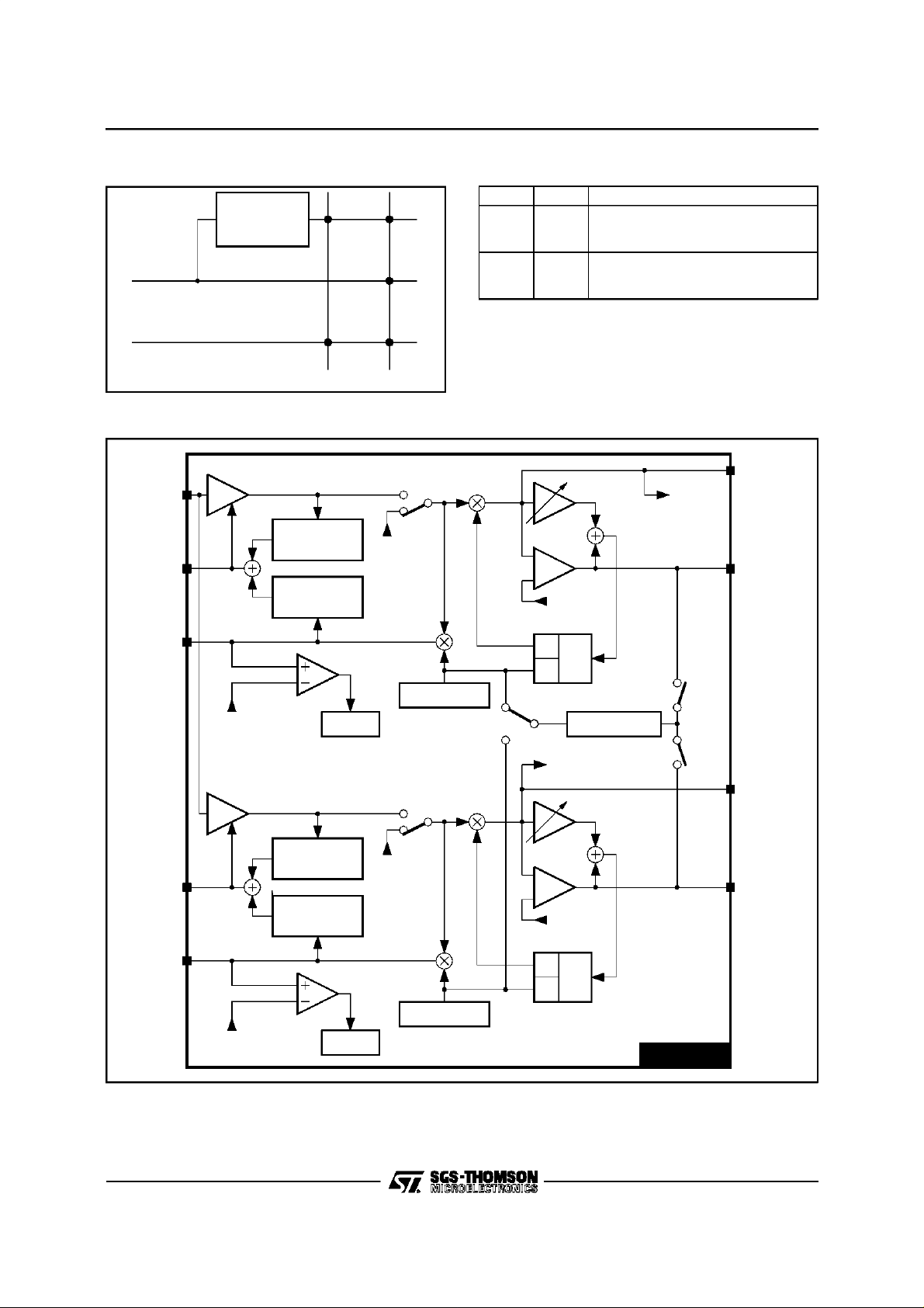
AUDIO SWITCHING
DEEMPHASIS
AUDIO PLL
AUDIO
+ ANRS
STV0042A
K
1a
K
5b
K
a
b
b
K
5c
a
b
b
K
2
1
2
1
2
ON
ON
ON
OFF
OFF
OFF
3
No ANRS, No De-emphasis
No ANRS, 50µs
No ANRS, 75µs
ANRS, No De-emphasis
ANRS, 50µs
ANRS, 75µs
AUX IN
K
1c
VOL OUT AUX OUT
FMDEMODULATION BLOCK DIAGRAM
FM IN
AGC R
AMPLKR
AGC
V
AGC
REF
LEVEL
DETECTOR1
LEVEL
DETECTOR2
Reg8 b4
Bias
Amp. Detect
K
5a
SW1
WATCHDOG
SW3
0042A-06.EPS
Phase
Detect
Phase
Detect
FM dev.
Select.
V
REF
90
VCO
0
SYNTHESIZER
AUDIOL
DETR
AUDIOR
CPUMP R
SW2
SW4
DETL
AGC L
AMPLKL
LEVEL
DETECTOR1
Bias
FM dev.
Select.
CPUMP L
LEVEL
DETECTOR2
V
REF
Amp. Detect
90
VCO
0
WATCHDOG
V
REF
Reg8 b0
STV0042A
0042A-07.EPS
7/24

STV0042A
CIRCUITDESCRIPTION
1 - VideoSection
Thecompositevideo is first set to a standard level
by means of a 64 step gain controlledamplifier. In
thecasethat themodulationisnegative,an inverter
canbe switchedin.
One of two different external video de-emphasis
networks (for instance PAL and NTSC) is selectable by an integrated bus controlledswitch.
Then energy dispersal is removed by a sync tip
clamping circuit, which is used on all inputs to a
video switching matrix, thus making sure that no
DC steps occur when switching video sources.
The matrix can be used to feedvideo to and from
decoders,VCR’sand TV’s.
Additionaly all the video outputs are tristate type
(high impedance mode is supported), allowing a
simple parallel connections to the scarts (Twin
tunerapplications).
2 - Audio Section
Thetwoaudio channelsare totallyindependentexceptfor thepossibilitygivento outputonbothchannelsonlyone of the selectedinputaudiochannels.
To allow a very cost effective application, each
channel uses PLL demodulation. Neither external
complexfilter nor ceramicfiltersare needed.
The frequency of the demodulated subcarrier is
chosenby a frequencysynthesizerwhich sets the
frequency of the internal local oscillator by comparing its phase with the internally generated
reference. When the frequency is reached, the
microprocessor switches in the PLL and the demodulationstarts.Atanymomentthe microprocessor can read fromthe device(watchdog registers)
the actual frequencyto which the PLLis locked.It
canalsoverifythatacarrierispresentatthe wanted
frequency(by reading AMPLKstatus bit)thanks to
a synchronous amplitude detector, which is also
usedfor the audio input AGC.
In order to maintain constant amplitude of the
recovered audio regardless of variationsbetween
satellitesor subcarriers,the PLLloop gain may be
programmedfrom 56 values.
Any frequency deviation can be accomodated
(from ±30kHztill ±400kHz).
In thetypical application,theSTV0042Aofferstwo
audiode-emphasis75µsand 50µs. Whenrequired
a J17 de-emphasis can be implemented by using
specificapplicationdiagram(seeApplicationNote:
AN838, Chapter 4.2).
Adynamic noise reduction system (ANRS) is integrated into the STV0042A using a lowpass filter,
the cut-off frequency of which is controlled by the
amplitude of the audio after insertion of a bandpass filter.
Twotypes of audio outputs are provided: one is a
fixed 1V
2V
RMS
and the other is a gain controlled
RMS
max. The control range being from +12dB
to-26.75dBwith1.25dBsteps.Thisoutputcanalso
be muted.
A matrixis implementedto feed audioto and from
decodersVCR’s and TV’s.
Noise reduction system and de-emphasis can be
insertedor by-passedthroughbus control.
Also all the audio outputs are tristate-type (high
impedancemodeis supported),allowinga simple
parallel connections to the scarts (Twin tuner
applications).
3 - Others
A22kHz tone is generatedfor LNB control.
It isselectableby bus controland availableon one
of the two pins connected to the external video
de-emphasisnetworks.
By means of the I
2
C bus there is the possibility to
drive the ICs into a low power consumption mode
with a ctive audio and video matrixes. Independantly from the main power mode, each individualaudioand video outputcan bedrivento high
impedancemode.
8/24
 Loading...