

SGS Thomson Microelectronics STU9NA60 Datasheet
N - CHANNEL ENHANCEMENT MODE
FAST POWER MOS TRANSISTOR
TYPE V
DSS
STU9NA60 600 V < 0.8 Ω 9 A
R
DS(on)
I
STU9NA60
PRELIMINARY DATA
D
■ TYPICAL R
■ EFFICIENT AND RELAIBLE MOUNTING
DS(on)
= 0.68 Ω
THROUGH CLIP
■ ± 30V GATE TO SOURCE VOLTA GE RATING
■ 100% AVALANCHE TESTED
■ GATE CH ARGE MINIMIZED
■ REDUCED THRESHOLD VO LTA GE SPREA D
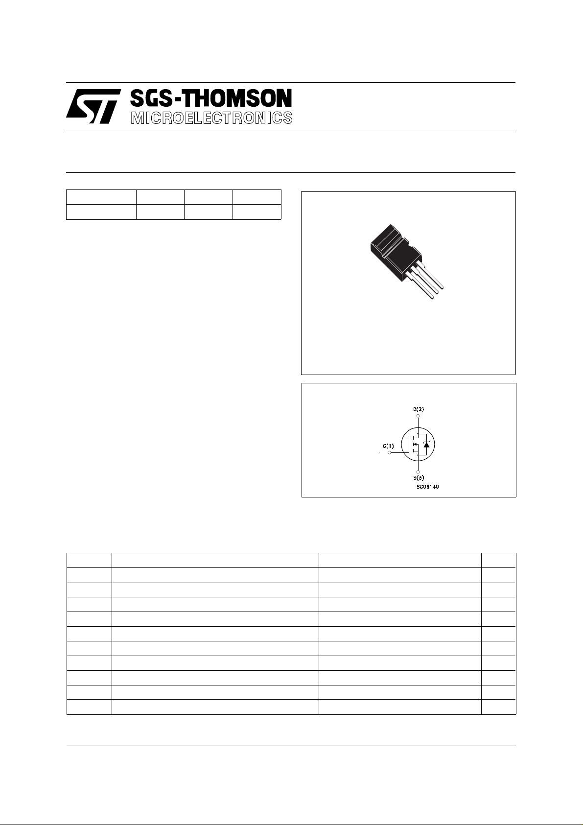
DESCRIPTION
The Max220
TM
package is a new high volume
power package exibiting the same footprint as the
industry standard TO-220, but designed to
accomodate much larger silicon chips, normally
supplied in bigger packages. The increased die
capacity makes the device ideal to reduce
component count in multiple paralleled TO-220
designs and save board space with respect to
larger packages.
APPLICATIONS
■ HIGH CURRENT, HIGH SPE ED SWI TCHING
■ SWITCH MODE P OW ER SUP P LIE S (S MP S)
■ DC-AC CONVERTERS FOR WELDING
EQUIPMENT AND UNINTERRUPTIBLE
POWER SU PP LIE S (UPS)
3
2
1
Max220
TM
INTERNAL SCHEMATIC DIAGRAM
ABSOL UT E MAXIMU M RATINGS
Symbol Parameter Value Unit
V
V
V
I
DM
P
T
(•) Pulse width limited by safe operating area
March 1996
Drain-source Voltage (VGS = 0) 600 V
DS
Drain- gate Voltage (RGS = 20 kΩ) 600 V
DGR
Gate-source Voltage ± 30 V
GS
I
Drain Current (continuous) at Tc = 25 oC9A
D
I
Drain Current (continuous) at Tc = 100 oC 5.7 A
D
(•) Drain Current (pulsed) 36 A
Total Dissipation at Tc = 25 oC 145 W
tot
Derating Factor 1.16 W/
Storage Temperature -65 to 150
stg
T
Max. Operating Junction Temperature 150
j
o
C
o
C
o
C
1/5
STU9NA60
THERMAL DATA
R
thj-case
Rthj-amb
R
thc-si n k
T
Thermal Resistance Junction-case Max
Thermal Resistance Junction-ambient Max
Thermal Resistance Case-sink Typ
Maximum Lead Temperature For Soldering Purpose
l
AVALANCHE CHARACTERI S TICS
Symbol Parameter Max Value Unit
I
AR
E
E
I
AR
Avalanche Current, Repetitive or Not-Repetitive
(pulse width limited by T
Single Pulse Avalanche Energy
AS
(starting T
Repetitive Avalanche Energy
AR
= 25 oC, ID = IAR, V
j
(pulse width limited by T
max, δ < 1%)
j
DD
max, δ < 1%)
j
Avalanche Current, Repetitive or Not-Repetitive
(T
= 100 oC, pulse width limited by Tj max, δ < 1%)
c
= 50 V)
0.86
30
0.1
300
9A
405 mJ
16.2 mJ
5.7 A
o
C/W
oC/W
o
C/W
o
C
ELECTRICAL CHARACTERISTICS (T
= 25 oC unless otherwise specified)
case
OFF
Symbol Parameter Test Conditions Min. Typ. Max. Unit
V
(BR)DSS
Drain-source
ID = 250 µA V
= 0 600 V
GS
Breakdown Voltage
I
DSS
I
GSS
Zero Gate Voltage
Drain Current (V
GS
Gate-body Leakage
Current (V
DS
= 0)
= 0)
= Max Rating
V
DS
V
= Max Rating x 0.8 Tc = 125 oC
DS
= ± 30 V ± 100 nA
V
GS
250
1000µAµA
ON (∗)
Symbol Parameter Test Conditions Min. Typ. Max. Unit
V
GS(th)
R
DS(on)
I
D(on)
Gate Threshold Voltage V
Static Drain-source On
Resistance
= VGS ID = 250 µA 2.25 3 3.75 V
DS
VGS = 10 V ID = 4.5 A
V
= 10 V ID = 4.5 A Tc = 100oC
GS
On State Drain Current VDS > I
V
= 10 V
GS
D(on)
x R
DS(on)max
0.68 0.8
1.6
9A
DYNAMIC
Symbol Parameter Test Conditions Min. Typ. Max. Unit
g
(∗) Forward
fs
Transconductance
C
C
C
Input Capacitance
iss
Output Capacitance
oss
Reverse Transfer
rss
Capacitance
VDS > I
V
DS
x R
D(on)
DS(on)max
= 25 V f = 1 MHz V
ID = 4.5 A 5 6.6 S
= 0 1770
GS
230
65
2300
300
85
Ω
Ω
pF
pF
pF
2/5
 Loading...