

SGS Thomson Microelectronics STU16NC50 Datasheet
STU16NC50
N-CHANNEL 500V - 0.22Ω - 16A Max220
PowerMesh™II MOSFET
TYPE V
DSS
R
DS(on)
I
D
STU16NC50 500V < 0.27Ω 16 A
■ TYPICAL R
■ EXTREMELY HIGH dv /d t CAPABILITY
■ 100% AVALANCHE TESTED
■ NEW HIGH VOLTAGE BENCHMARK
■ GATE CHARGE MINIMIZED
(on) = 0.22Ω
DS
DESCRIPTION
The PowerMESH
generation of MESH OVERLAY
™II is the evolution of the first
™. The layout re-
finements introduced greatly improve the Ron*area
figure of merit while keeping the device at the lea ding edge for what concerns swithing speed, gate
charge and ruggedness.
APPLICATIONS
■ HIGH CURRENT, HIGH SPEED SWITCHING
■ UNINTERRUPTIBLE POWER SUPPLIES (UPS)
■ DC-AC CONVERTERS FOR TELECOM,
INDUSTRIAL, AND LIGHTING EQUIPMENT
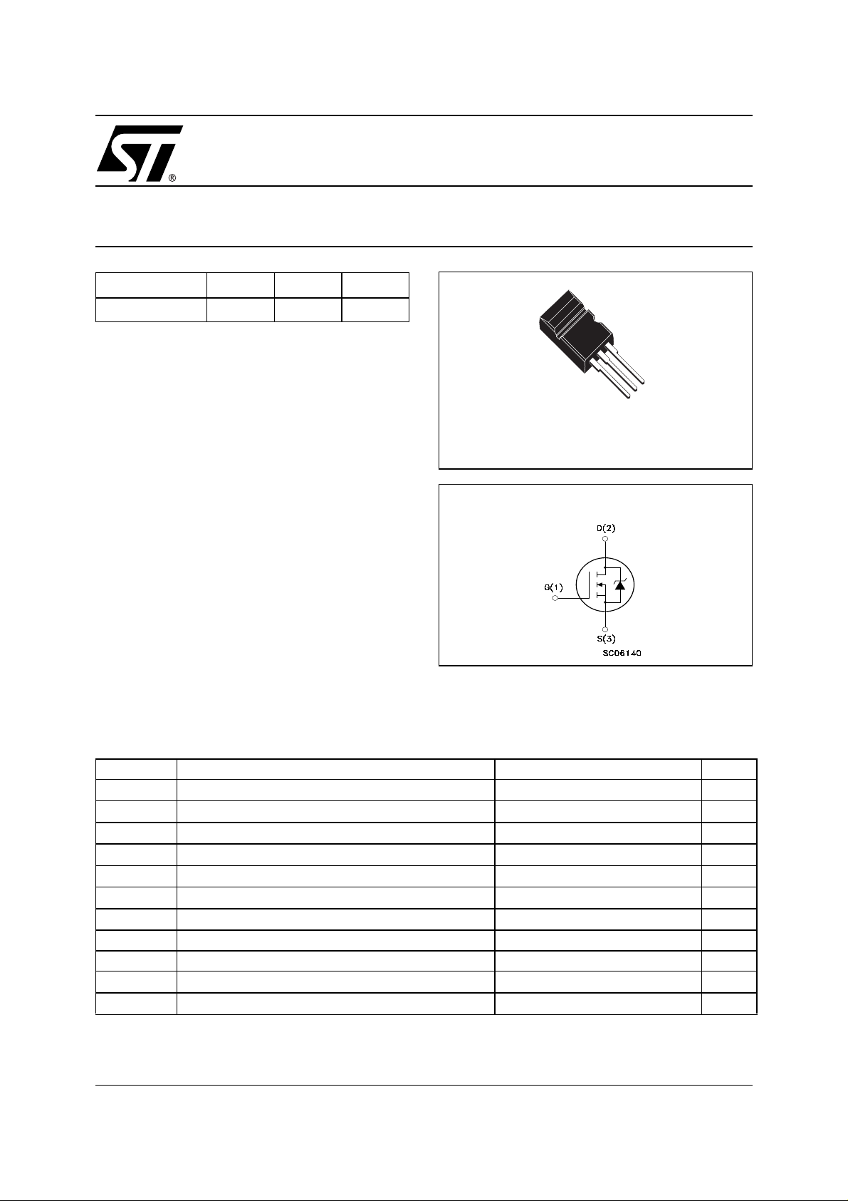
3
2
1
Max220
INTERNAL SCHEMATIC DIAGRAM
ABSOLUTE MAXIMUM RATINGS
Symbol Parameter Value Unit
V
DS
V
DGR
V
GS
I
D
I
D
I
DM
P
TOT
dv/dt(1) Peak Diode Recovery voltage slope 3 V/ns
T
stg
T
j
(•)Pu l se width limite d by safe operat i ng area
Drain-source Voltage (VGS = 0)
Drain-gate Voltage (RGS = 20 kΩ)
500 V
500 V
Gate- source Voltage ±30 V
Drain Current (continuos) at TC = 25°C
Drain Current (continuos) at TC = 100°C
(●)
Drain Current (pulsed) 64 A
Total Dissipation at TC = 25°C
16 A
10 A
160 W
Derating Factor 1.28 W/°C
Storage Temperature –65 to 150 °C
Max. Operating Junction Temperature 150 °C
(1)ISD ≤16A, di/dt ≤100A/µs, VDD ≤ V
(BR)DSS
, Tj ≤ T
JMAX.
1/8October 2001
STU16NC50
THERMA L D ATA
Rthj-case Thermal Resistance Junction-case Max 0.78 °C/W
Rthj-amb Thermal Resistance Junction-ambient Max 62.5 °C/W
T
l
AVALANCHE CHARACTERISTICS
Symbol Parameter Max Value Unit
I
AR
E
AS
ELECTRICAL CHARACTERISTICS (TCASE = 25 °C UNLESS OTHERWISE SPECIFIED)
OFF
Symbol Parameter Test Conditions Min. Typ. Max. Unit
V
(BR)DSS
I
DSS
I
GSS
Maximum Lead Temperature For Soldering Purpose 300 °C
Avalanche Current, Repetitive or Not-Repetitive
(pulse width limited by T
max)
j
Single Pulse Avalanche Energy
(starting T
Drain-source
= 25 °C, ID = IAR, VDD = 50 V)
j
ID = 250 µA, VGS = 0 500 V
16 A
1000 mJ
Breakdown Voltage
Zero Gate Voltage
Drain Current (V
GS
Gate-body Leakage
Current (V
DS
= 0)
= 0)
V
= Max Rating
DS
V
= Max Rating, TC = 125 °C
DS
V
= ±30V ±100 nA
GS
1µA
50 µA
(1)
ON
Symbol Parameter Test Conditions Min. Typ. Max. Unit
V
GS(th)
R
DS(on)
Gate Threshold Voltage
Static Drain-source On
V
= VGS, ID = 250 µA
DS
VGS = 10V, ID = 9A
234V
0.22 0.27 Ω
Resistance
DYNAMIC
Symbol Parameter Test Conditions Min. Typ. Max. Unit
g
fs
C
iss
C
oss
C
rss
Forward Transconductance VDS > I
I
=9A
D
Input Capacitance
V
DS
Output Capacitance 410 pF
Reverse Transfer
Capacitance
D(on)
x R
DS(on)max,
= 25V, f = 1 MHz, VGS = 0
18 S
2980 pF
58 pF
2/8
STU16NC50
ELECTRICAL CHARACTERISTICS (CONTINUED)
SWITCHING ON
Symbol Parameter Test Conditions Min. Typ. Max. Unit
t
d(on)
t
Q
Q
Q
gd
r
g
gs
Turn-on Delay Time
Rise Time
Total Gate Charge
Gate-Source Charge 14.7 nC
Gate-Drain Charge 41.7 nC
SWITCHING OFF
Symbol Param eter Test Conditions Min. Typ. Max. Unit
t
r(Voff)
t
t
f
c
Off-voltage Rise Time
Fall Time 30 ns
Cross-over Time 58 ns
SOURCE DRAIN DIODE
Symbol Parameter Test Conditions Min. Typ. Max. Unit
I
SD
I
SDM
V
SD
t
rr
Q
rr
I
RRM
Note: 1. Pulsed: Pul se duration = 300 µs, duty cycle 1.5 %.
2. Pulse width l i m i t ed by safe operat i ng area.
Source-drain Current 16 A
(2)
Source-drain Current (pulsed) 64 A
(1)
Forward On Voltage
Reverse Recovery Time
Reverse Recovery Charg e 5 µ C
Reverse Recovery Curren t 21 A
= 250V, ID = 10 A
V
DD
RG= 4.7Ω VGS = 10V
(see test circuit, Figure 3)
V
= 400V, ID = 20 A,
DD
VGS = 10V
VDD = 400V, ID = 20 A,
RG= 4.7Ω, V
GS
= 10V
(see test circuit, Figure 5)
I
= 18.4 A, VGS = 0
SD
= 20 A, di/dt = 100A/µs,
I
SD
V
= 100V, Tj = 150°C
DD
(see test circuit, Figure 5)
29 ns
21 ns
95 128 nC
14 ns
1.6 V
480 ns
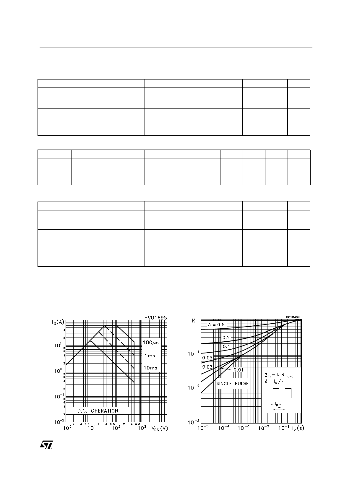
Safe Operating Area Thermal Impedance
3/8
 Loading...