

SGS Thomson Microelectronics STU13NB60 Datasheet
STU13NB60
N-CHANNEL ENHANCEMENT MODE
PowerMESH MOSFET
PRELIMINARY DATA
TYPE V
DSS
R
DS(on)
I
D
ST U1 3NB60 600 V < 0.45 Ω 12.6 A
■ TYPICALR
■ EXTREMELY HIGH dv/dt CAPABILITY
■ 100% AVALANCHETESTED
■ VERYLOW INTRINSICCAPACITANCES
■ GATECHARGEMINIMIZED
■ ± 30V GATE TO SOURCE VOLTAGERATING
DS(on)
=0.4 Ω
DESCRIPTION
Using the latest high voltage MESH OVERLAY
process, SGS-Thomson has designed an
advanced family of power MOSFETs with
outstanding performances. The new patent
pending strip layout coupled with the Company’s
proprietary edge termination structure, gives the
lowest R
per area, exceptional avalanche
DS(on)
and dv/dt capabilities and unrivalled gate charge
and switching characteristics.
APPLICATIONS
■ SWITCHMODEPOWER SUPPLIES(SMPS)
■ DC-ACCONVERTERS FOR WELDING
EQUIPMENTAND UNINTERRUPTIBLE
POWERSUPPLIESAND MOTORDRIVE
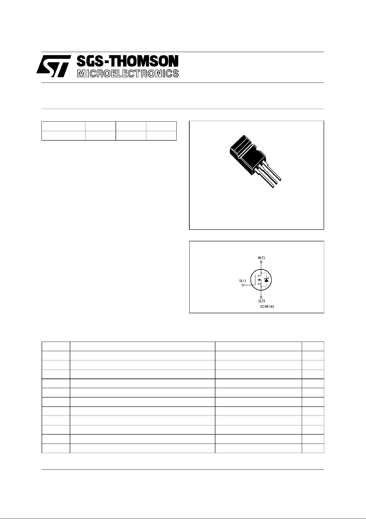
3
2
1
Max220
INTERNAL SCHEMATIC DIAGRAM
ABSOLUTE MAXIMUM RATINGS
Symb o l Para meter Value Uni t
V
V
V
I
DM
P
dv/dt(
T
(•) Pulse width limited by safe operating area (1)ISD≤13A, di/dt ≤ 200 A/µs,VDD≤ V
October 1997
This ispreliminary information on a new productnow in development or undergoing evaluation. Details are subject to changewithout notice.
Drain-source Voltage (VGS=0) 600 V
DS
Drain- gate Voltage (RGS=20kΩ)
DGR
Gat e- source Vo lt age ± 30 V
GS
I
Drain Cur rent (c on t inuous) at Tc=25oC12.6A
D
I
Drain Cur rent (c on t inuous) at Tc=100oC7.9A
D
600 V
(•) Drain Current (pul sed) 50.4 A
Tot al Dissip at ion at Tc=25oC160W
tot
Derating F actor 1.28 W/
1) Peak Diode Rec ov er y vo lt age s l ope 4.5 V/ns
Sto rage Temper ature -65 to 150
stg
T
Max. Operating Ju nct ion T e m peratur e 150
j
,Tj≤T
(BR)DSS
JMAX
o
C
o
C
o
C
1/6
STU13NB60
THERMAL DATA
R
thj-case
Rthj-a mb
R
thc-sin k
T
AVALANCHE CHARACTERISTICS
Symbol Para met e r Max Value Uni t
I
AR
E
Ther mal Resist ance Junction- case Max
Ther mal Resist ance Junction- ambient Max
Ther mal Resist ance Case-sink T y p
Maximum Lead Tem per a t u re F o r Soldering Purpos e
l
Avalanche Cur re nt , Repetiti v e or Not-Re petitive
(pulse width limited by T
Single Pulse Avalanche Energy
AS
(starting T
=25oC, ID=IAR,VDD=50V)
j
max, δ <1%)
j
0.78
62.5
0.5
300
12.6 A
800 mJ
o
C/W
oC/W
o
C/W
o
C
ELECTRICAL CHARACTERISTICS (T
=25oC unlessotherwise specified)
case
OFF
Symbol Parameter Test Cond itions Min. Typ . Max. Unit
V
(BR)DSS
I
DSS
I
GSS
Drain-sourc e
Breakdown V oltage
Zer o Gat e V o lt age
Drain Current (V
GS
Gat e-body Leaka ge
Current (V
DS
=0)
=0)
=250µAVGS=0
I
D
o
@100
V
V
V
C
=MaxRating
DS
=MaxRating Tc=125oC
DS
= ± 30 V
GS
600 V
1
50
± 100 nA
ON (∗)
Symbol Parameter Test Cond itions Min. Typ. Max. Unit
V
GS(th )
Gate Threshold
V
DS=VGSID
=250µA
345V
Voltage
R
DS(on)
Stati c D rain-source On
VGS=10V ID=6.3 A 0.4 0.45 Ω
Resistance
I
D(on)
On State Drain Curre nt VDS>I
D(on)xRDS(on)max
12.6 A
VGS=10V
DYNAMIC
Symbol Parameter Test Cond itions Min. Typ. Max. Unit
g
(∗)Forward
fs
Tr ansconductanc e
C
C
C
Input Capac i t an c e
iss
Out put C apa c itance
oss
Reverse Transf er
rss
Capa cit an c e
VDS>I
D(on)xRDS(on)maxID
=6.3 A 6 9 S
VDS=25V f=1MHz VGS= 0 2950
370
33
3840
480
43
µA
µA
pF
pF
pF
2/6
 Loading...