

SGS Thomson Microelectronics STSJ25NF3LL Datasheet
STSJ25NF3LL
N-CHANNEL 30V - 0.009Ω - 25A PowerSO-8™
LOW GATE CHARGE STripFET™ II POWER MOSFET
TYPE V
STSJ25NF3LL 30 V < 0.011 Ω 25 A
■ IMPROVED JUNCTION-CASE THERMAL
DSS
R
DS(on)
I
D
RESISTANCE
■ TYPICAL R
■ TYPICAL Q
■ CONDUCTION LOSSES REDUCED
■ SWITCHING LOSSES REDUCED
(on) = 0.009Ω
DS
= 21 nC
g
DESCRIPTION
This Power MOSFET is t he latest development of
STMicroelectronics unique “Single Feature Size
™”
strip-based process. This silicon, housed in thermally improved SO-8 package, exhibits optimal on-resistance versus gate charge trade-off plus lower
.
R
thj-c
APPLICATIONS
■ SPECIFICALLY DESIGNED AND OPTIMISED
FOR HIGH EFFICIENCY CPU CORE DC/DC
CONVERTERS FOR MOBILE PCs
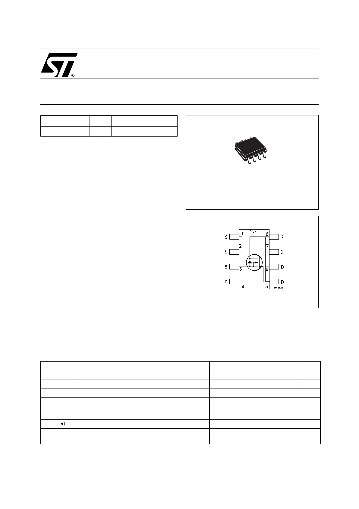
PowerSO-8
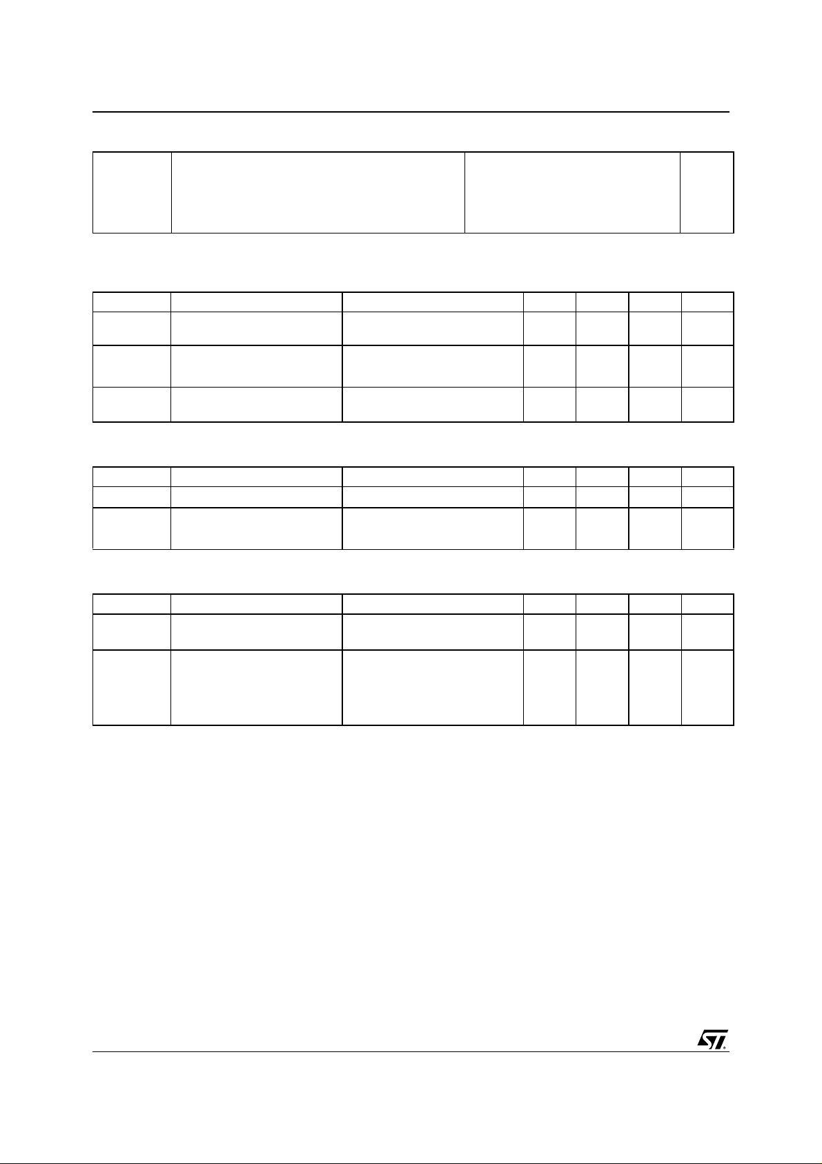
INTERNAL SCHEMATIC DIAGRAM
DRAIN CONTACT ALSO ON THE BACKSIDE
ABSOLUTE MAXIMUM RATINGS
Symbol Parameter Value Unit
V
DS
V
DGR
V
GS
I
D
I
DM
P
TOT
(●) Pulse width limited by safe operating area
Drain-source Voltage (VGS = 0)
Drain-gate Voltage (RGS = 20 kΩ)
Gate- source Voltage ± 16 V
Drain Current (continuous) at TC = 25°C (*)
Drain Current (continuous) at TA = 25°C (#)
Drain Current (continuous) at T
(l)
Drain Current (pulsed) 100 A
Total Dissipation at TC = 25°C
Total Dissipation at TA = 25°C (#)
= 100°C
C
(*)Value li m ited by wir es bonding
30 V
30 V
25
12
16
70
3
A
A
A
W
W
1/8March 2002
STSJ25NF3LL
THERMA L D ATA
Rthj-c Thermal Resistance Junction-case Max 1.8 °C/W
Rthj-amb Thermal Resistance Junction-ambient Max (#) 42 °C/W
T
j
T
stg
(#) When mounted on 1inc h² FR4 Board, 2oz of Cu, t ≤ 10 sec.
Max. Operating Junction Temperature 150 °C
Storage Temperature – 55 to 150 °C
ELECTRICAL CHARACTERISTICS (T
= 25 °C UNLESS OTHERWISE SPECIFIED)
CASE
OFF
Symbol Parameter Test Conditions Min. Typ. Max. Unit
V
(BR)DSS
Drain-source
ID = 250 µA, VGS = 0 30 V
Breakdown Voltage
ON
I
I
GSS
(1)
DSS
Zero Gate Voltage
Drain Current (V
GS
Gate-body Leakage
Current (V
DS
= 0)
= 0)
V
= Max Rating
DS
V
= Max Rating, TC = 125 °C
DS
V
= ± 16V ±100 nA
GS
1µA
10 µA
Symbol Parameter Test Conditions Min. Typ. Max. Unit
V
V
GS(th)
R
DS(on)
Gate Threshold Voltage
Static Drain-source On
Resistance
= VGS, ID = 250µA
DS
VGS = 10 V, ID = 12.5 A
VGS = 4.5 V, ID = 12.5 A
1V
0.009 0.011 Ω
0.011 0.013 Ω
DYNAMIC
Symbol Parameter Test Conditions Min. Typ. Max. Unit
(1) Forward Transconductance VDS > I
g
fs
C
iss
C
oss
C
rss
Input Capacitance
Output Capacitance 500 pF
Reverse Transfer
Capacitance
ID= 5.5 A
V
DS
x R
D(on)
DS(on)max,
= 25 V, f = 1 MHz, VGS = 0
20 S
1700 pF
115 pF
2/8

STSJ25NF3LL
ELECTRICAL CHARACTERISTICS (CONTINUED)
SWITCHING ON
Symbol Parameter Test Conditions Min. Typ. Max. Unit
V
t
d(on)
Q
Q
Q
t
r
g
gs
gd
Turn-on Delay Time
Rise Time 60 ns
Total Gate Charge
Gate-Source Charge
Gate-Drain Charge
SWITCHING OFF
Symbol Parameter Test Conditions Min. Typ. Max. Unit
t
d(off)
t
f
Turn-off-Delay Time
Fall Time
SOURCE DRAIN DIODE
Symbol Parameter Test Conditions Min. Typ. Max. Unit
I
SD
I
SDM
VSD (2)
t
rr
Q
rr
I
RRM
Note: 1. Pulsed: Pu l se duration = 300 µs, duty cyc l e 1.5 %.
2. Pulse width li mited by safe operating ar ea.
Source-drain Current 25 A
(1)
Source-drain Current (pulsed) 100 A
Forward On Voltage
Reverse Recovery Time ISD = 25 A, di/dt = 100A/µs,
= 15 V, ID = 12.5 A
DD
R
= 4.7Ω VGS = 4.5 V
G
(see test circuit, Figure 3)
VDD = 15 V, ID = 25 A,
VGS = 4.5 V
VDD = 24 V, ID = 12.5 A,
RG=4.7Ω, V
GS
= 4.5 V
(see test circuit, Figure 3)
ISD = 25 A, VGS = 0
VDD = 15 V, Tj = 150°C
(see test circuit, Figure 5)
47 ns
21
28
10
8.4
34
24
1.3 V
40
52
2.4
nC
nC
nC
ns
ns
ns
nC
A
Thermal Imp e danceSafe Operating Area
3/8
 Loading...