

SGS Thomson Microelectronics STS9NF30L Datasheet
STS9NF30L
N-CHANNEL 30V - 0.015
LOW GATE CHARGE STripFET POWER MOSFET
TYPE V
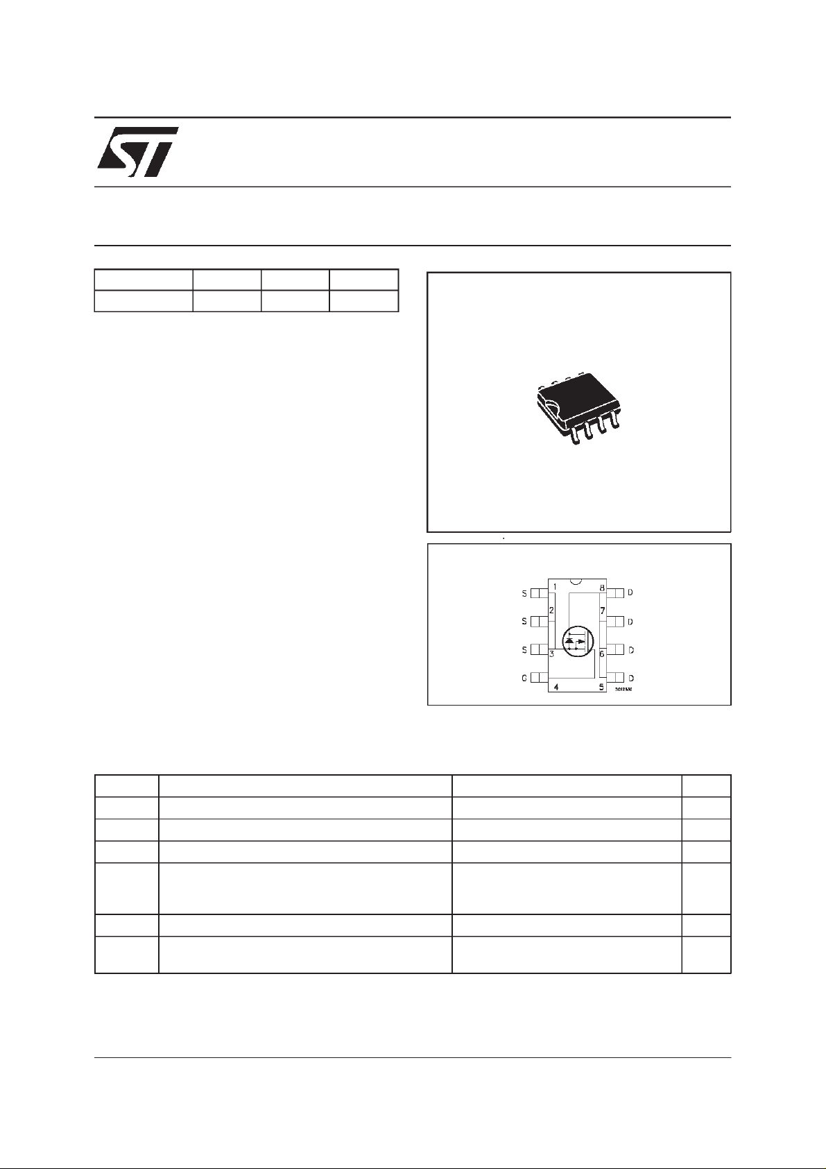
ST S9NF30L 30 V < 0.020 Ω 9A
■ TYPICALR
■ TYPICALQ
■ OPTIMAL R
■ CONDUCTIONLOSSESREDUCED
■ SWITCHINGLOSSESREDUCED
DSS
= 0.018 Ω @ 4.5V
DS(on)
= 9 nC @ 4.5V
g
DS(on)xQg
DESCRIPTION
This applicationspecific Power Mosfet is the third
generation of STMicroelectronics unique ”Single
Feature Size” strip-based process. The resulting transistor shows the best trade-off between
on-resistance and gate charge. When used as
high and low side in buck regulators, it gives the
best performancein termsof both conductionand
switching losses. This is extremely important for
motherboardswhere fast switching and high efficiencyare of paramount importance.
R
DS(on)
TRADE-OFF
I
D
Ω
- 9A SO-8
PRELIMINARY DATA
SO-8
INTERNAL SCHEMATIC DIAGRAM
APPLICATIONS
■ SPECIFICALLYDESIGNED AND
OPTIMISEDFOR HIGH EFFICIENCYCPU
CORE DC/DC CONVERTERSFOR MOBILE
PCs
ABSOLUTE MAXIMUM RATINGS
Symb o l Parameter Value Unit
V
V
V
I
DM
P
(•) Pulse width limited by safe operating area
Drain-source Voltage (VGS=0) 30 V
DS
Drain- gate Voltage (RGS=20kΩ)30V
DGR
Gate-s ource Voltage ± 20 V
GS
Drain Curr ent (co nt inu ous ) at T c = 25oC
I
D
Drain Curr ent (co nt inu ous ) at T
(•) Drain Curr ent (puls ed) 36 A
Tot al Dis sipation at Tc=25oC 2.5 W
tot
=100oC
c
9
5.6
A
A
May 2000
1/6
STS9NF30L
THERMAL DATA
R
thj-amb
T
T
(*)Mountedon FR-4 board (t ≤ 10sec)
(*)T hermal Resistance Junction-ambie nt
Maximum Ope ra t ing Junct i on Temperatur e
j
stg
St orage Te m pe ra t ure
50
150
-65 to 150
o
C/W
o
o
C
C
ELECTRICAL CHARACTERISTICS
=25oC unless otherwisespecified)
(T
case
OFF
Symbol Parameter Test Conditions Min. Typ. Max. Unit
V
(BR)DSS
Drain-source
ID=250µAVGS=0 30 V
Break dow n V o lt age
ON (
I
DSS
I
GSS
∗)
Zero Gate Voltage
Drain Cur re nt ( V
GS
Gat e- bod y L eakage
Current (V
DS
=0)
=0)
V
=MaxRating
DS
=MaxRating Tc=125oC
V
DS
= ± 20 V ± 100 nA
V
GS
1
10
Symbol Parameter Test Conditions Min. Typ. Max. Unit
V
GS(th)
R
DS(on)
I
D(on)
Gate Threshold Voltage VDS=VGSID= 250 µA1 V
Sta t ic Drain -s ource O n
Resistance
VGS=10V ID=4A
=4.5V ID=4A
V
GS
On State Drain Current VDS>I
D(on)xRDS(on)max
0.015
0.018
9A
0.020
0.024
VGS=10V
DYNAMIC
Symbol Parameter Test Conditions Min. Typ. Max. Unit
g
(∗)Forward
fs
Tr ansc on duc tance
C
C
C
Input Capac i t ance
iss
Out put Capacitance
oss
Reverse Tr ansfer
rss
Capacit a nc e
VDS>I
D(on)xRDS(on)maxID
=5.5A 10 S
VDS=25V f=1MHz VGS= 0 V 750
270
60
µA
µA
Ω
Ω
pF
pF
pF
2/6
 Loading...