

STS8NFS30L
STripFET
MAIN PRODUCT CHARACTERISTICS
MOSFET
SCHOTTKY
DESCRIPTION:
This product associates the latest low voltage
StripFET
Schottky diode. Such configuration is extremely
versatile in implementing, a large variety of DCDC converters for printers, portable equipment,
and cellularphones.
MOSFETABSOLUTE MAXIMUM RATINGS
Symbol Parameter Value Unit
in n-channel version to a low drop
V
V
V
I
DM
P
Drain-source Volta ge (VGS=0) 30 V
DS
Drain- gate Volta ge (RGS=20kΩ)30V
DGR
Gat e- sour c e Volt age ± 20 V
GS
I
Drain Current ( cont inuous ) a t Tc=25oC8A
D
I
Drain Current ( cont inuous ) a t Tc= 100oC5A
D
(•) Drain Current (pulsed) 32 A
Tot al D iss ip at ion at Tc=25oC2.5W
tot
MOSFET PLUS SCHOTTKY RECTIFIER
V
DSS
30 V <0.022 Ω 8A
I
F(AV)
3A 30V 0.51V
R
DS(on)
V
RRM
V
F(MAX)
I
D
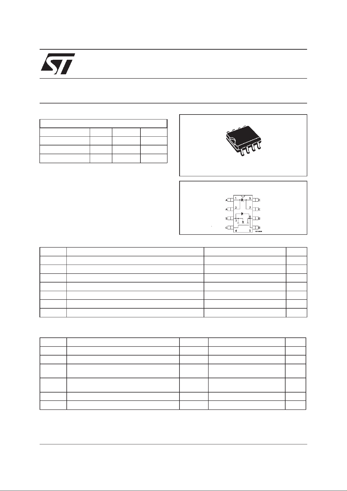
SO-8
INTERNAL SCHEMATIC DIAGRAM
N - CHANNEL 30V - 0.018Ω - 8A S0-8
SCHOTTKY ABSOLUTE MAXIMUM RATINGS
Symbol Parameter Valu e Unit
V
I
F(RMS)
I
F ( AV)
I
FSM
I
RSM
dv/d t Critical Rat e Of Rise O f Revers e V olt age 10000 V/µs
(•) Pulse width limited by safeoperatingarea
December 1999
Repetitive Peak Rev er se Vol t age 30 V
RRM
RMS Forwa r d Current 20 A
Aver ag e F orw ar d Current TL=125oC
δ =0.5
Surge N on Repetitive F orward Current tp= 1 0 ms
Sinusoidal
Non Repet it i v e Peak Rever se Curr e nt tp= 100 µs1 A
3A
75 A
1/8
STS8NFS30L
THERMAL DATA
R
thj-amb
R
thj-amb
T
T
(*) Thermal Resist ance Junction-ambient MOSFE T
(*) Thermal Resist ance Junction- ambientSCHOTT KY
Sto rage Temperature Range Maxim u m
stg
Junct ion T em per ature
j
(*)
mounted on FR-4 board (steady state)
50
100
-65 t o 150
150
o
C/W
o
C/W
o
o
C
C
MOSFETELECTRICAL CHARACTERISTICS
=25oC unless otherwisespecified)
(T
case
OFF
Symbol Parameter Test Conditions Min. Typ. Max. Unit
V
(BR)DSS
Drain-source
ID=250µAVGS=0 30 V
Break dow n Voltage
I
DSS
I
GSS
Zero Gate Volta ge
Drain Current ( V
GS
Gat e- bod y Leakage
Current (V
DS
=0)
=0)
V
=MaxRating
DS
=MaxRating Tc= 125oC
V
DS
V
=± 20 V
GS
1
10
100 nA
±
ON(∗)
Symbol Parameter Test Conditions Min. Typ. Max. Unit
V
GS(th)
R
DS(on)
I
D(on)
Gate Threshold Voltage VDS=VGSID= 250 µA11.62.5V
Sta t ic Drain-s ource On
Resistance
VGS=10V ID=4A
=4.5V ID=4A
V
GS
On State Drain Current VDS>I
D(on)xRDS(on)max
0.018
0.021
8A
0.022
0.026ΩΩ
VGS=10V
DYNAMIC
Symbol Parameter Test Conditions Min. Typ. Max. Unit
g
(∗)Forward
fs
Tr ansc on duc tance
C
C
C
Input Capaci t ance
iss
Out put Capac it ance
oss
Reverse Transfer
rss
Capacit a nc e
VDS>I
D(on)xRDS(on)maxID
=4 A 10 S
VDS=25V f=1MHz VGS= 0 1050
250
85
µ
µA
pF
pF
pF
A
2/8

STS8NFS30L
ELECTRICAL CHARACTERISTICS
(continued)
SWITCHING ON
Symbol Parameter Test Conditions Min. Typ. Max. Unit
t
d(on)
t
Tur n-on Delay Time
Rise T ime
r
VDD=15V ID=4A
R
G
=4.7
VGS=4.5V
Ω
22
60
(Resis t iv e Load, s ee f ig. 3)
Q
Q
Q
Tot al Gate C harge
g
Gat e- Source Charg e
gs
Gate-Drain Charge
gd
VDD=24V ID=8A VGS= 4. 5 V 17.5
4
7
23 nC
SWITCHING OFF
Symbol Parameter Test Conditions Min. Typ. Max. Unit
t
d(off)
Tur n-of f Dela y T im e
t
Fall Time
f
VDD=15V ID=4A
=4.7Ω VGS=4.5V
R
G
42
10
(Resis t iv e Load, s ee f ig. 3)
t
r(Voff)
t
t
Off-vo ltage Rise T im e
Fall Time
f
Cross-over T ime
c
VDD=24V ID=8A
=4.7Ω VGS=4.5V
R
G
(Indu ct iv e Load, se e fig. 5)
11
12
25
SOURCEDRAINDIODE
Symbol Parameter Test Conditions Min. Typ. Max. Unit
I
SD
I
SDM
V
SD
t
Q
I
RRM
(∗) Pulsed: Pulse duration = 300 µs, duty cycle 1.5 %
(•) Pulse width limited by safe operating area
Source-drain Current
(•)
Source-drain Current
8
32
(pulsed)
(∗)ForwardOnVoltage ISD=8A VGS=0 2 V
Reverse Recovery
rr
Time
Reverse Recovery
rr
ISD=8A di/dt=100A/µs
=20V Tj= 150oC
V
DD
(see test circuit, figure 5)
50
40
Charge
Reverse Recovery
1.6
Current
ns
ns
nC
nC
ns
ns
ns
ns
ns
A
A
ns
nC
Α
SCHOTTCKY STATIC ELETTRICALCHARACTERISTICS
Symbol Parameter Test Conditions Min. Typ. Max. Unit
I
(∗) Reversed Leakage
R
Current
V
(∗) For ward Voltage drop TJ=25oCI
F
TJ=25oCV
=125oCV
T
J
=125oCI
T
J
=30V
R
=30V 0.03
R
=3A
F
=3A 0.38
F
0.2
100
0.51
0.46
mA
mA
V
V
3/8

STS8NFS30L
SafeOperating Area
OutputCharacteristics
ThermalImpedance
TransferCharacteristics
Transconductance
4/8
Static Drain-source On Resistance

STS8NFS30L
Gate Chargevs Gate-sourceVoltage
NormalizedGate ThresholdVoltage vs
Temperature
CapacitanceVariations
NormalizedOn Resistancevs Temperature
Source-drainDiode ForwardCharacteristics
5/8

STS8NFS30L
Fig. 1:
UnclampedInductive Load Test Circuit
Fig. 3: SwitchingTimes Test CircuitsFor
ResistiveLoad
Fig. 2:
UnclampedInductive Waveform
Fig. 4: Gate Charge test Circuit
Fig. 5:
Test CircuitFor InductiveLoad Switching
And DiodeRecovery Times
6/8

SO-8 MECHANICALDATA
STS8NFS30L
DIM.
MIN. TYP. MAX. MIN. TYP. MAX.
A 1.75 0.068
a1 0.1 0.25 0.003 0.009
a2 1.65 0.064
a3 0.65 0.85 0.025 0.033
b 0.35 0.48 0.013 0.018
b1 0.19 0.25 0.007 0.010
C 0.25 0.5 0.010 0.019
c1 45 (typ.)
D 4.8 5.0 0.188 0.196
E 5.8 6.2 0.228 0.244
e 1.27 0.050
e3 3.81 0.150
F 3.8 4.0 0.14 0.157
L 0.4 1.27 0.015 0.050
M 0.6 0.023
S 8 (max.)
mm inch
0016023
7/8

STS8NFS30L
Information furnished is believedto be accurate and reliable. However, STMicroelectronics assumes no responsibility forthe consequences
of use of such information nor for any infringement of patents or other rights of third parties which may result from its use. No license is
granted by implication or otherwise under any patent or patent rights of STMicroelectronics. Specification mentioned in this publicationare
subjecttochange without notice. This publication supersedes and replaces all information previously supplied.STMicroelectronics products
are not authorized for use as critical components in life support devices or systemswithout express written approval of STMicroelectronics.
The ST logo is a trademark of STMicroelectronics
1999STMicroelectronics – Printed in Italy – All Rights Reserved
STMicroelectronics GROUP OF COMPANIES
Australia - Brazil - China - Finland - France - Germany - Hong Kong - India - Italy - Japan - Malaysia - Malta - Morocco -
8/8
Singapore - Spain - Sweden - Switzerland - United Kingdom - U.S.A.
http://www.st.com
.
 Loading...