


STS8DNF3LL
DUAL N-CHANNEL 30V - 0.017 Ω - 8A SO-8
LOW GATE CHARGE STripFET™ II POWER MOSFET
TYPE
V
DSS
STS8DNF3LL 30 V <0.020
■ TYPICAL R
■ OPTIMAL R
■ CONDUCTION LOSSES REDUCED
■ SWITCHING LOSSES REDUCED
(on) = 0.017Ω
DS
(on) x Qg TRADE-OFF @ 4.5V
DS
R
DS(on)
I
D
8 A
Ω
DESCRIPTION
This application speci fic Power MOSFET is the second
generation of STMicro electronis unique "Single Feature
Size™" strip-based process. The resulting transistor
shows the best trade-off between on-resistance and gate
charge. When used as high and low side in buck
regulators, it gives the be st perfor manc e in terms of both
conduction and switching losses. This is extremely
important for motherboards where fast switching and
high efficiency are of paramount importance.
APPLICATIONS
■ SPECIFICALL Y D ESIGNED AND OPTIMISED
FOR HIGH EFFICIENCY CPU CORE DC/DC
CONVERTERS FOR MOBILE PC
S
SO-8
INTERNAL SCHEMATIC DIAGRAM
ABSOLUTE MAXIMUM RATINGS
Symbol Parameter Value Unit
V
DS
V
DGR
V
GS
I
D
I
DM
P
(
Pulse widt h l i m i ted by safe operating area.
•)
.
Drain-source Voltage (VGS = 0)
Drain-gate Voltage (RGS = 20 kΩ)
30 V
30 V
Gate- source Voltage ± 16 V
Drain Current (continuous) at TC = 25°C
8
Single Operation
Drain Current (continuous) at T
= 100°C
C
5
Single Operation
(
•)
Drain Current (pulsed) 32 A
Total Dissipation at TC = 25°C Dual operating
tot
Total Dissipation at T
= 25°C Single operating
C
2
1.6
A
W
W
1/8October 2002
STS8DNF3LL
THERMA L D ATA
Rthj-amb
T
T
stg
(*)
When mounted on FR-4 board with 0.5 in2 pad of Cu.
(*)Thermal Resistance Junction-ambient Single Operating
Thermal Operating Junction-ambient
j
Storage Temperature
Dual Operating
78
62.5
150
-55 to 150
°C/W
°C/W
°C
°C
ELECTRICAL CHARACTERISTICS (T
= 25 °C unless otherwise specified)
case
OFF
Symbol Parameter Test Conditions Min. Typ. Max. Unit
I
= 250 µA, VGS = 0
D
V
= Max Rating
DS
V
= Max Rating TC = 125°C
DS
V
= ± 16 V
GS
30 V
1
10
±100 nA
ON
V
(BR)DSS
I
DSS
I
GSS
(*)
Drain-source
Breakdown Voltage
Zero Gate Voltage
Drain Current (V
GS
Gate-body Leakage
Current (V
DS
= 0)
= 0)
Symbol Parameter Test Conditions Min. Typ. Max. Unit
V
V
GS(th)
R
DS(on)
Gate Threshold Voltage
Static Drain-source On
Resistance
= VGS I
DS
= 10 V ID = 4 A
V
GS
V
= 4.5 V ID = 4 A
GS
= 250 µA
D
1V
0.017
0.020
0.020
0.024
DYNAMIC
Symbol Parameter Test Conditions Min. Typ. Max. Unit
(*)
g
fs
C
iss
C
oss
C
rss
Forward Transconductance
Input Capacitance
Output Capacitance
Reverse Transfer
Capacitance
V
=15 V ID=4 A
DS
= 25V, f = 1 MHz, VGS = 0
V
DS
12.5 S
800
250
60
µA
µA
Ω
Ω
pF
pF
pF
2/8
STS8DNF3LL
ELECTRICAL CHARACTERISTICS (continued)
SWITCHING ON
Symbol Parameter Test Conditions Min. Typ. Max. Unit
= 15 V ID = 4 A
t
d(on)
Turn-on Delay Time
t
r
Rise Time
V
DD
R
= 4.7 Ω VGS = 4.5 V
G
(Resistive Load, Figure 1)
Q
g
Q
gs
Q
gd
Total Gate Charge
Gate-Source Charge
Gate-Drain Charge
= 15 V ID= 8 A VGS= 5 V
V
DD
(see test circuit, Figure 2)
SWITCHING OFF
Symbol Parameter Test Conditions Min. Typ. Max. Unit
= 15 V ID = 4 A
t
d(off)
Turn-off Delay Time
t
f
Fall Time
V
DD
R
= 4.7Ω, V
G
GS
= 4.5 V
(Resistive Load, Figure 1)
SOURCE DRAIN DIODE
Symbol Parameter Test Conditions Min. Typ. Max. Unit
I
SD
I
SDM
V
SD
t
rr
Q
rr
I
RRM
(*)
Pulsed: P ul se duration = 300 µs, duty cy cle 1.5 %.
(
•)Pulse width limited by safe operating area.
Source-drain Current
(•)
Source-drain Current (pulsed)
(*)
Forward On Voltage
Reverse Recovery Time
Reverse Recovery Charge
Reverse Recovery Current
I
= 8 A VGS = 0
SD
= 8 A di/dt = 100A/µs
I
SD
V
= 15 V Tj = 150°C
DD
(see test circuit, Figure 3)
18
32
12.5
3.2
4.5
21
11
23
17
1.5
17 nC
8
32
1.2 V
ns
ns
nC
nC
ns
ns
A
A
ns
nC
A
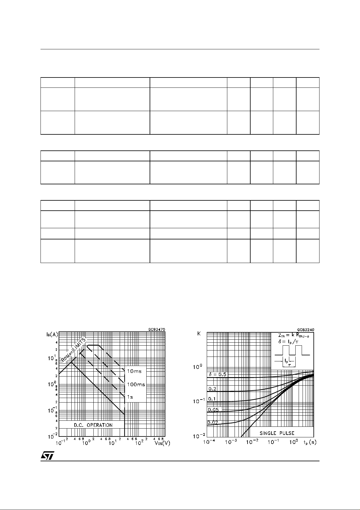
Safe Operating Area Thermal Impedance
3/8

STS8DNF3LL
Output Characteristics Transfer Characteristics
Transconductance Static Drain-source On Resistance
Gate Charge vs Gate-source Voltage Capacitance Variations
4/8

STS8DNF3LL
Normalized Gate Threshold Voltage vs Temperature Normalized on Resistance vs Temperature
Source-drain Diode Forward Characteristics Normalized Breakdown Voltage vs Temperature.
. .
. .
5/8

STS8DNF3LL
Fig. 1: Switching Times Test Circuits For Resistive
Load
Fig. 3: Test Circuit For Diode Recovery Behaviour
Fig. 2: Gate Charge test Circuit
6/8

SO-8 MECHANICAL DATA
STS8DNF3LL
DIM.
MIN. TYP. MAX. MIN. TYP. MAX.
A1.750.068
a1 0.1 0.25 0.003 0.009
a2 1.65 0.064
a3 0.65 0.85 0.025 0.033
b 0.35 0.48 0.013 0.018
b1 0.19 0.25 0.007 0.010
C 0.25 0.5 0.010 0.019
c1 45 (typ.)
D 4.8 5.0 0.188 0.196
E 5.8 6.2 0.228 0.244
e1.27 0.050
e3 3.81 0.150
F 3.8 4.0 0.14 0.157
L 0.4 1.27 0.015 0.050
M0.60.023
S 8 (max.)
mm inch
0016023
7/8

STS8DNF3LL
Information furnished is believed to be accurate and reliable. However, STMicroelectronics assumes no responsibility for the consequences
of use of such information nor for any infringement of patents or other rights of third parties which may result from its use. No license is granted
by implic ation or oth erwise under any patent or pat ent rights of STMicroelectronic s. Specifications mentioned in this pub lication are subject
to change without notice. This publication supersedes and replaces all information previously supplied. STMicroelectronics products are not
authorized for use as critical comp onents in life support devi ces or systems wi thout express written approval of STMi croelectr onics.
The ST logo is registered trademark of STMicroelectronics
2002 STMi croelectr oni cs - All Righ ts Reserved
All other na m es are the prop erty of their res pective ow ners.
Australi a - Brazil - Canada - China - F i nl and - France - Germany - Hong Kong - Ind ia - Israel - Italy - Japan - Malay sia - Malta - Morocco -
Singap ore - Spain - Sweden - Switzerland - Uni ted Kingdom - United States.
STMicroelectronics GROUP OF COMPANIES
http:// www.st.com
8/8
 Loading...