

SGS Thomson Microelectronics STS7PF30L Datasheet
STS7PF30L
P-CHANNEL 30V - 0.016Ω -7ASO-8
STripFET™ II POWER MOSFET
PRELIMINARY DATA
TYPE V
STS7PF30L 30 V < 0.021 Ω 7A
■ TYPICAL R
■ STANDARD OUTLINE FOR EASY
DSS
(on) = 0.016Ω
DS
R
DS(on)
I
D
AUTOMATED SURFACE MOUNT ASSEMBLY
■ LOW THRESHOLD DRIVE
DESCRIPTION
This Power Mosfet is the latest development of STMicroelectronics unique “Single Feature Size
™”
strip-based proc es s . The resulting transistor shows
extremely high packing density for low on-resistance, rugged avalanche characteristics and less
critical alignment stepstherefore a remarkable manufacturing reproducibility.
APPLICATIONS
■ BATTERY MANAGEMENT IN NOMADIC
EQUIPMENT
■ POWER MANAGEMENT IN CELLULAR
PHONES
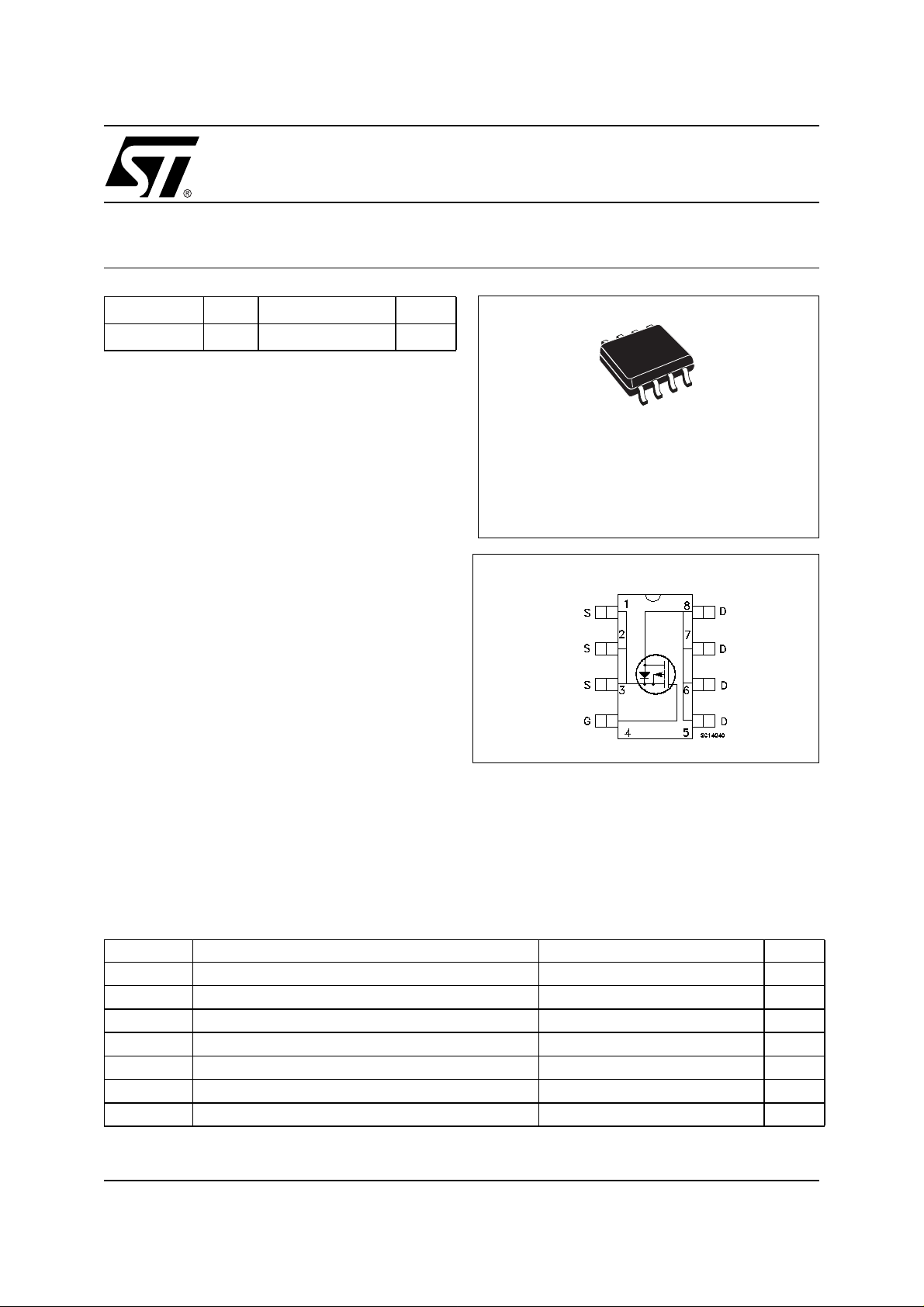
SO-8
INTERNAL SCHEMATIC DIAGRAM
ABSOLUTE MAXIMUM RATINGS
Symbol Parameter Value Unit
V
DS
V
DGR
V
GS
I
D
I
D
I
DM
P
TOT
(●) Pulse width limited by safe operating area
December 2002
Drain-source Voltage (VGS=0)
Drain-gate Voltage (RGS=20kΩ)
Gate- source Voltage ±20 V
Drain Current (continuous) at TC= 25°C
Drain Current (continuous) at TC= 100°C
Drain Current (pulsed) 28 A
Total Dissipation at TC= 25°C
Note: For the P-CHANNEL MOSFET actual polarity of voltages and
30 V
30 V
7A
4.4 A
2.5 W
current has to be reversed
1/6
STS7PF30L
THERMAL DATA
Rthj-amb(#) Thermal Re sistance Junction-ambient Max 50 °C/W
Tj Maxim um Lead Temperature For Soldering Purpose Typ 150 °C
T
stg
(#) When mounted on 1 inch2FR4 Board, 2 oz of Cu and t ≤ 10s
ELECTRICAL CHARACTERISTICS (TJ= 25 °C UNLESS OTHERRWISE SPECIFIED)
OFF
Symbol Parameter Test Conditions Min. Typ. Max. Unit
V
(BR)DSS
I
DSS
I
GSS
ON (1)
Symbol Parameter Test Conditions Min. Typ. Max. Unit
V
GS(th)
R
DS(on)
Storage Temperature –55 to 150 °C
Drain-source
ID= 250 µA, VGS= 0 30 V
Breakdown Voltage
Zero Gate Voltage
Drain Current (V
GS
=0)
Gate-body Lea kage
Current (V
DS
=0)
Gate Threshold Voltage
Static Drain-source On
Resistance
V
= Max Rating
DS
V
= Max Rating , TC= 125 °C
DS
V
= ± 20V ±100 nA
GS
V
DS=VGS,ID
VGS=10V,ID= 3.5A
= 4.5V, ID= 3.5A
V
GS
= 250µA
1 1.6 2.5 V
0.011 0.016 0.021 Ω
0.016 0.022 0.028 Ω
1µA
10 µA
DYNAMIC
Symbol Parameter Test Conditions Min. Typ. Max. Unit
g
fs
C
iss
C
oss
C
rss
Forward Transconductanc e VDS=10V,ID= 3.5A 16 S
V
Input Capacitance
=25V,f=1MHz,VGS=0
DS
2600 pF
Output Capacitance 523 pF
Reverse Transfer
174 pF
Capacitance
2/6
 Loading...