

STS7NF60L
N-CHANNEL 60V - 0.017 Ω - 7.5A S O-8
STripFET™ II POWER MOSFET
TYPE
V
DSS
STS7NF60L 60 V < 0.0195
■ TYPICAL R
■ STANDARD OUTLIN E FO R EASY
(on) = 0.017 Ω
DS
R
DS(on)
I
D
7.5 A
Ω
AUTOMATED SURFACE MOUNT ASSEMBLY
■ LOW THRESHOLD DRIVE
DESCRIPTION
This Power MOSFET is the latest dev elo pment of
STMicroelectronis unique "Single Feature Size™"
strip-based process. The resulting transistor
shows extremely high packing density for low onresistance, rugged avalanche characteristics and
less critical alignment steps therefore a remarkable manufacturing reproducibility.
APPLICATIONS
■ DC MOTOR DRIVE
■ DC-DC CONVERTERS
■ BATTERY MANAGEMENT IN NOMADIC
EQUIPMENT
■ POWER MANAGEMENT IN
PORTABLE/DESKTOP PCs
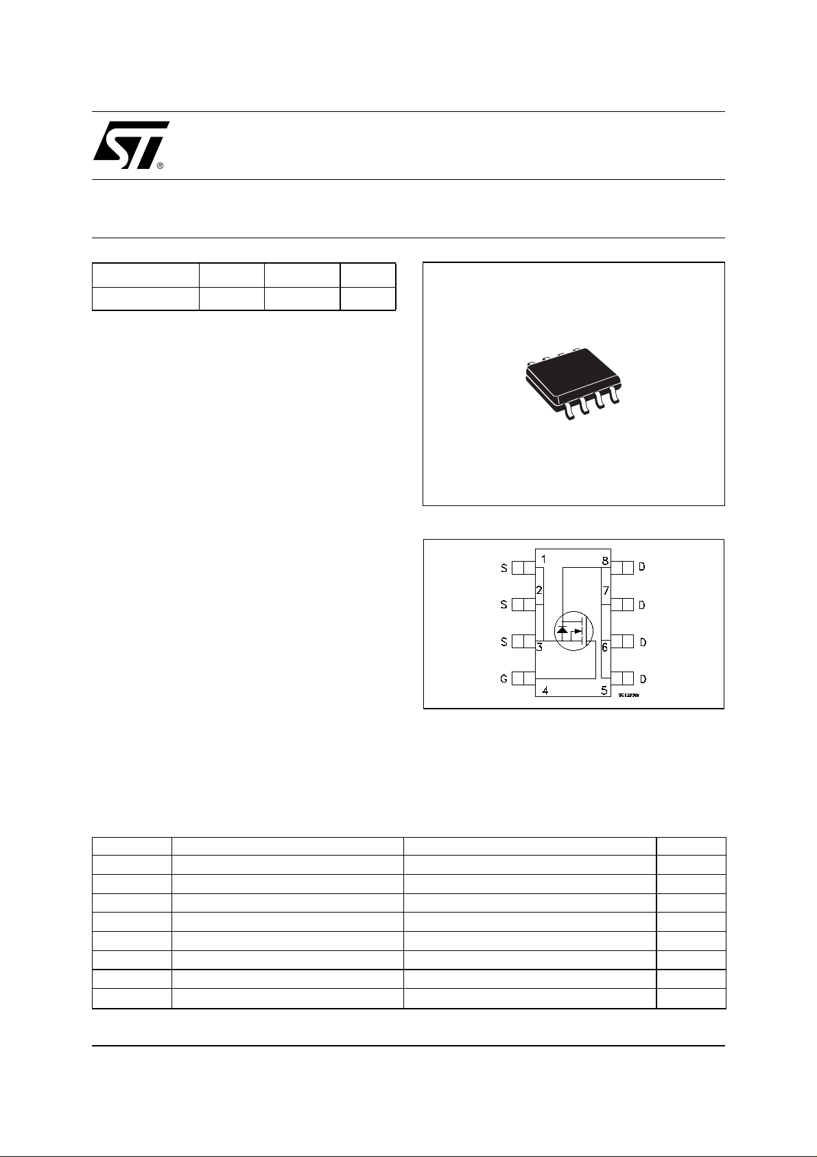
SO-8
INTERNAL SCHEMATIC DIAGRAM
ABSOLUTE MAXIMUM RATINGS
Symbol Parameter Value Unit
V
DS
V
DGR
V
GS
I
D
I
D
(
I
DM
P
tot
E
AS
(
Pulse width limited by safe operating area. (1) Starting Tj = 25 oC, ID = 7.5 A VDD = 30 V
•)
.
Drain-source Voltage (VGS = 0)
Drain-gate Voltage (RGS = 20 kΩ)
60 V
60 V
Gate- source Voltage ± 16 V
Drain Current (continuous) at TC = 25°C
Drain Current (continuous) at TC = 100°C
•)
Drain Current (pulsed) 30 A
Total Dissipation at TC = 25°C
(1)
Single Pulse Avalanche Energy 350 mJ
7.5 A
4.7 A
2.5 W
1/8April 2002
STS7NF60L
THERMA L D ATA
Rthj-amb(#)
T
T
stg
(#)
When Mounted on 1 inch
Thermal Resistance Junction-ambient
Maximum Operating Junction Temperature
j
Storage Temperature
2
FR-4 board, 2 oz of Cu and t [ 10 sec.
Max 50
150
-55 to 150
°C/W
°C
°C
ELECTRICAL CHARACTERISTICS (T
= 25 °C unless otherwise specified)
case
OFF
Symbol Parameter Test Conditions Min. Typ. Max. Unit
I
= 250 µA, VGS = 0
D
V
= Max Rating
DS
V
= Max Rating TC = 125°C
DS
V
= ± 16 V
GS
60 V
1
10
±100 nA
ON
V
(BR)DSS
I
DSS
I
GSS
(*)
Drain-source
Breakdown Voltage
Zero Gate Voltage
Drain Current (V
GS
Gate-body Leakage
Current (V
DS
= 0)
= 0)
Symbol Parameter Test Conditions Min. Typ. Max. Unit
V
V
GS(th)
R
DS(on)
Gate Threshold Voltage
Static Drain-source On
Resistance
= VGS I
DS
= 10 V ID = 3.5 A
V
GS
V
= 5 V ID = 3.5 A
GS
= 250 µA
D
1V
0.017
0.019
0.0195
0.0215
DYNAMIC
Symbol Parameter Test Conditions Min. Typ. Max. Unit
V
g
fs
C
iss
C
oss
C
rss
Forward Transconductance
Input Capacitance
Output Capacitance
Reverse Transfer
Capacitance
= 15 V ID= 3.5 A
DS
= 25V, f = 1 MHz, VGS = 0
V
DS
13 S
1700
300
100
µA
µA
Ω
Ω
pF
pF
pF
2/8
STS7NF60L
ELECTRICAL CHARACTERISTICS (continued)
SWITCHING ON
Symbol Parameter Test Conditions Min. Typ. Max. Unit
t
d(on)
t
r
Q
g
Q
gs
Q
gd
(*)
Turn-on Delay Time
Rise Time
Total Gate Charge
Gate-Source Charge
Gate-Drain Charge
= 30 V ID = 3.5 A
V
DD
R
= 4.7 Ω VGS = 4.5 V
G
(Resistive Load, Figure 1)
= 48V ID 7.5A VGS=4.5V
V
DD
(see test circuit, Figure 2)
15
27
25
4.5
7
34 nC
ns
ns
nC
nC
SWITCHING OFF
(*)
Symbol Parameter Test Conditions Min. Typ. Max. Unit
t
d(off)
Turn-off Delay Time
t
f
Fall Time
V
DD
R
= 4.7Ω, V
G
GS
= 4.5 V
47
20
= 30 V ID = 3.5 A
(Resistive Load, Figure 1)
SOURCE DRAIN DIODE
(*)
Symbol Parameter Test Conditions Min. Typ. Max. Unit
I
SD
I
SDM
V
SD
t
rr
Q
rr
I
RRM
(*)
Pulse width [ 300 µs, duty cycle 1.5 %.
(
•)Pulse width limited by safe operating area.
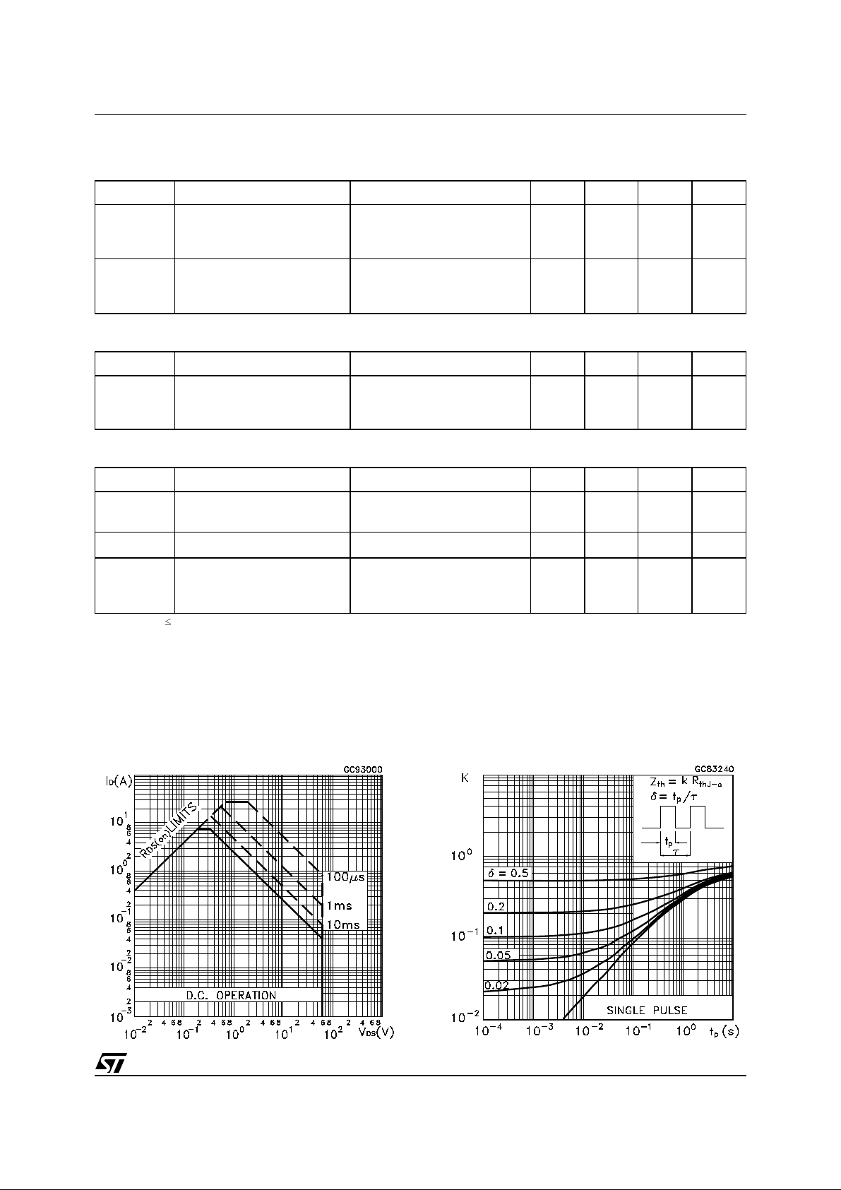
Saf e Operating Ar ea
Source-drain Current
(•)
Source-drain Current (pulsed)
Forward On Voltage
Reverse Recovery Time
Reverse Recovery Charge
Reverse Recovery Current
I
= 7.5 A VGS = 0
SD
=7.5 A di/dt = 100A/µs
I
SD
V
= 20 V Tj = 150°C
DD
(see test circuit, Figure 3)
Thermal Impedance
7.5
30
1.2 V
55
110
3.9
ns
ns
A
A
ns
nC
A
3/8

STS7NF60L
Output Characteristics Transfer Characteristics
Transconductance Static Drain-source On Resistance
Gate Charge vs Gate-source Voltage Capacitance Variations
4/8

STS7NF60L
Normalized Gate Threshold Voltage vs Temperature Normalized on Resistance vs Temperature
Source-drain Diode Forward Characteristics Normalized Breakdown Voltage vs Temperature
. .
5/8

STS7NF60L
Fig. 1: Unclamped Inductive Load Test CircuitFig. 1: Unclamped Inductive Load Test Circuit Fig. 2: Unc lamped I nduct ive Waveform
Fig. 3: Switching Times Test Circuits For Resistive
Load
Fig. 5: Test Circuit For Inductive Load Switching
And Diode Recovery Times
Fig. 4: Gate Charge test Circuit
6/8

SO-8 MECHANICAL DATA
STS7NF60L
DIM.
MIN. TYP. MAX. MIN. TYP. MAX.
A1.750.068
a1 0.1 0.25 0.003 0.009
a2 1.65 0.064
a3 0.65 0.85 0.025 0.033
b 0.35 0.48 0.013 0.018
b1 0.19 0.25 0.007 0.010
C 0.25 0.5 0.010 0.019
c1 45 (typ.)
D 4.8 5.0 0.188 0.196
E 5.8 6.2 0.228 0.244
e1.27 0.050
e3 3.81 0.150
F 3.8 4.0 0.14 0.157
L 0.4 1.27 0.015 0.050
M0.60.023
S 8 (max.)
mm inch
0016023
7/8

STS7NF60L
Information furnished is bel i eved to be accurate and reliable. How ever, STMicroel ectronics assumes no responsibility for the consequence s
of use of such information nor for any infringement of patents or other rights of third parties which may result from its use. No license is granted
by implic ation or otherwise under any patent or patent rights of STMic roelectroni cs . Specificati ons mentione d i n this public at ion are s ubject
to change without notice. This publication supersedes and replaces all information previously supplied. STMicroelectronics products are not
authorized for use as criti cal component s in l i fe support devi ces or systems wit hout express wri tten approval of STMicroelec t ro nics.
The ST log o i s registered tr ademark of STMicroelectronics
2002 STMi croelectronics - All Right s Reserved
All other names are the property of thei r respective ow ners.
Australi a - Brazil - Can ada - China - Finla nd - F rance - Germany - Hong Kong - India - Israel - Ita l y - Japan - Malays i a - M alta - Morocco -
Singapor e - S pai n - Sweden - Swit zerland - United K i ngdom - United States.
STMicroelect ro n ics GRO UP OF COMPANI ES
http://www.st.com
8/8
 Loading...