

SGS Thomson Microelectronics STS6DNF30V Datasheet
STS6DNF30V
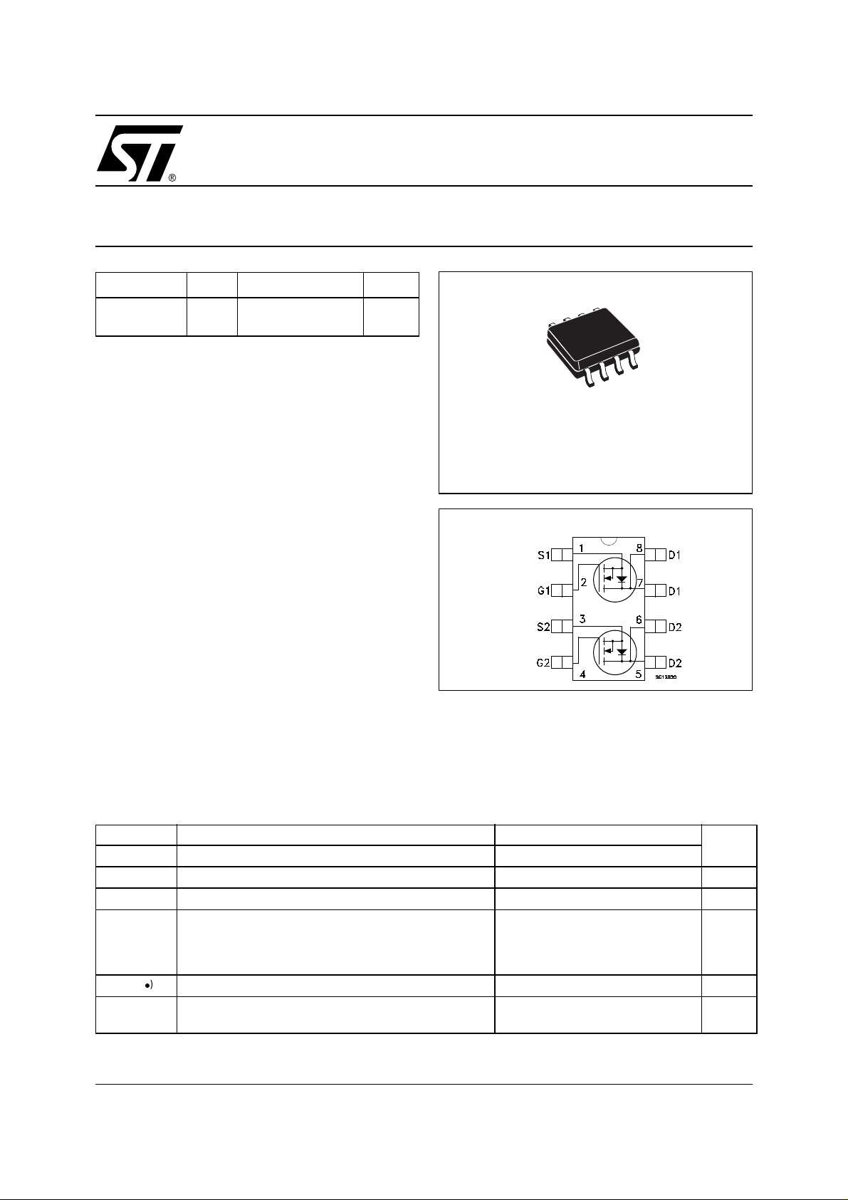
DUAL N-CHANNEL 30V - 0.026Ω - 6A SO-8
2.5V-DRIVE STripFET™ II POWER MOSFET
TYPE V
STS6DNF30V 30 V
■ TYPICAL R
■ TYPICAL R
■ ULTRA LOW THRESHOLD GATE DRIVE (2.5V)
■ STANDARD OUTLI NE FO R EASY
DSS
(on) = 0.026Ω (@4.5V)
DS
(on) = 0.030Ω (@2.5V)
DS
R
DS(on)
<0.030Ω (@4.5V)
<0.038Ω (@2.5V)
I
6 A
D
AUTOMATED SURFACE MOUNT ASSEMBLY
DESCRIPTION
This Power MOSFET is t he latest development of
STMicroelectronics unique “Single Feature Size
™”
strip-based process. The res ulting transistor sh ows
extremely high packing density for low on-resistance, rugged avalanche characteristics and less
critical alignment steps therefore a remarkable manufacturing reproducibility.
APPLICATIONS
■ BATTERY SAFETY UNIT IN NOMADIC
EQUIPMENT
■ DC-DC CONVERTERS
■ POWER MANAGEMENT IN PORTABLE/
DESKTOP PC
S
SO-8
INTERNAL SCHEMATIC DIAGRAM
ABSOLUTE MAXIMUM RATINGS
Symbol Parameter Value Unit
V
DS
V
DGR
V
GS
I
D
I
DM
P
TOT
(●) Pulse width limited by safe operating area
Drain-source Voltage (VGS = 0)
Drain-gate Voltage (RGS = 20 kΩ)
Gate- source Voltage ±12 V
Drain Current (continuos) at TC = 25°C
Single Operation
Drain Current (continuos) at T
Single Operation
(l)
Drain Current (pulsed) 24 A
Total Dissipation at TC = 25°C Dual Operation
Total Dissipation at TC = 25°C Single Operation
= 100°C
C
30 V
30 V
6
3.8
2
1.6
A
A
W
W
1/8July 2002
STS6DNF30V
THERMA L D ATA
Rthj-amb Thermal Resistance Junction-ambient Max Single Operation
Thermal Resistance Junction-ambient Max Dual Operation
T
j
T
stg
Max. Operating Junction Temperature 150 °C
Storage Temperature –65 to 150 °C
ELECTRICAL CHARACTERISTICS (TCASE = 25 °C UNLESS OTHERWISE SPECIFIED)
OFF
Symbol Parameter Test Conditions Min. Typ. Max. Unit
V
(BR)DSS
I
DSS
I
GSS
(1)
ON
Symbol Parameter Test Conditions Min. Typ. Max. Unit
V
GS(th)
R
DS(on)
Drain-source
Breakdown Voltage
Zero Gate Voltage
Drain Current (V
GS
= 0)
Gate-body Leakage
Current (V
DS
= 0)
Gate Threshold Voltage
Static Drain-source On
Resistance
ID = 250 µA, VGS = 0 30 V
V
= Max Rating
DS
V
= Max Rating, TC = 125 °C
DS
V
= ±12V ±100 nA
GS
V
= VGS, ID = 250µA
DS
0.6 V
VGS = 4.5 V, ID = 3 A
VGS = 2.5 V, ID = 3 A
78
62.5
1µA
10 µA
0.026 0.030 Ω
0.030 0.038 Ω
°C/W
°C/W
DYNAMIC
Symbol Parameter Test Conditions Min. Typ. Max. Unit
(1) Forward Transconductance VDS > I
g
fs
C
iss
C
oss
C
rss
Input Capacitance
Output Capacitance 180 pF
Reverse Transfer
Capacitance
ID= 3 A
V
DS
x R
D(on)
DS(on)max,
= 25 V, f = 1 MHz, VGS = 0
15 S
800 pF
32 pF
2/8
STS6DNF30V
ELECTRICAL CHARACTERISTICS (CONTINUED)
SWITCHING ON
Symbol Parameter Test Conditions Min. Typ. Max. Unit
V
t
d(on)
Q
Q
Q
t
r
gs
gd
Turn-on Delay Time
Rise Time 25 ns
Total Gate Charge
g
Gate-Source Charge
Gate-Drain Charge
SWITCHING OFF
Symbol Parameter Test Conditions Min. Typ. Max. Unit
t
d(off)
t
f
Turn-off-Delay Time
Fall Time
SOURCE DRAIN DIODE
Symbol Parameter Test Conditions Min. Typ. Max. Unit
I
SD
I
SDM
VSD (1)
t
rr
Q
rr
I
RRM
Note: 1. Pulsed: Pu l se duration = 300 µs, duty c ycle 1.5 %.
2. Pulse width li mited by safe operating area.
Source-drain Current 6 A
(2)
Source-drain Current (pulsed) 24 A
Forward On Voltage
Reverse Recovery Time
Reverse Recovery Charge
Reverse Recovery Current
= 15 V, ID = 3 A
DD
R
= 4.7Ω VGS = 2.5V
G
(see test circuit, Figure 3)
= 15 V, ID = 6 A,
V
DD
VGS = 2.5 V
VDD = 10 V, ID = 3 A,
RG=4.7Ω, V
GS
= 2.5 V
(see test circuit, Figure 3)
ISD = 6 A, VGS = 0
= 6 A, di/dt = 100A/µs,
I
SD
V
= 15 V, Tj = 150°C
DD
(see test circuit, Figure 5)
20 ns
6.8
9.5
2
3.4
32
13
1.2 V
25
21
1.7
nC
nC
nC
ns
ns
ns
nC
A
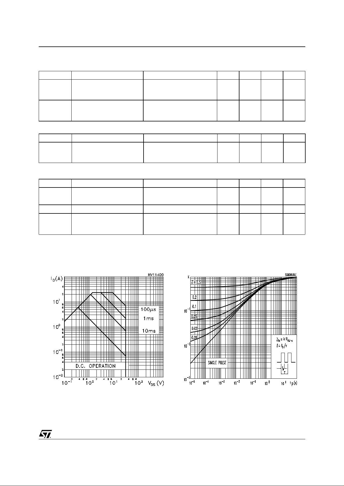
Safe Operating Area Thermal Impedance
3/8
 Loading...