

SGS Thomson Microelectronics STS6DNF30L Datasheet
STS6DNF30L
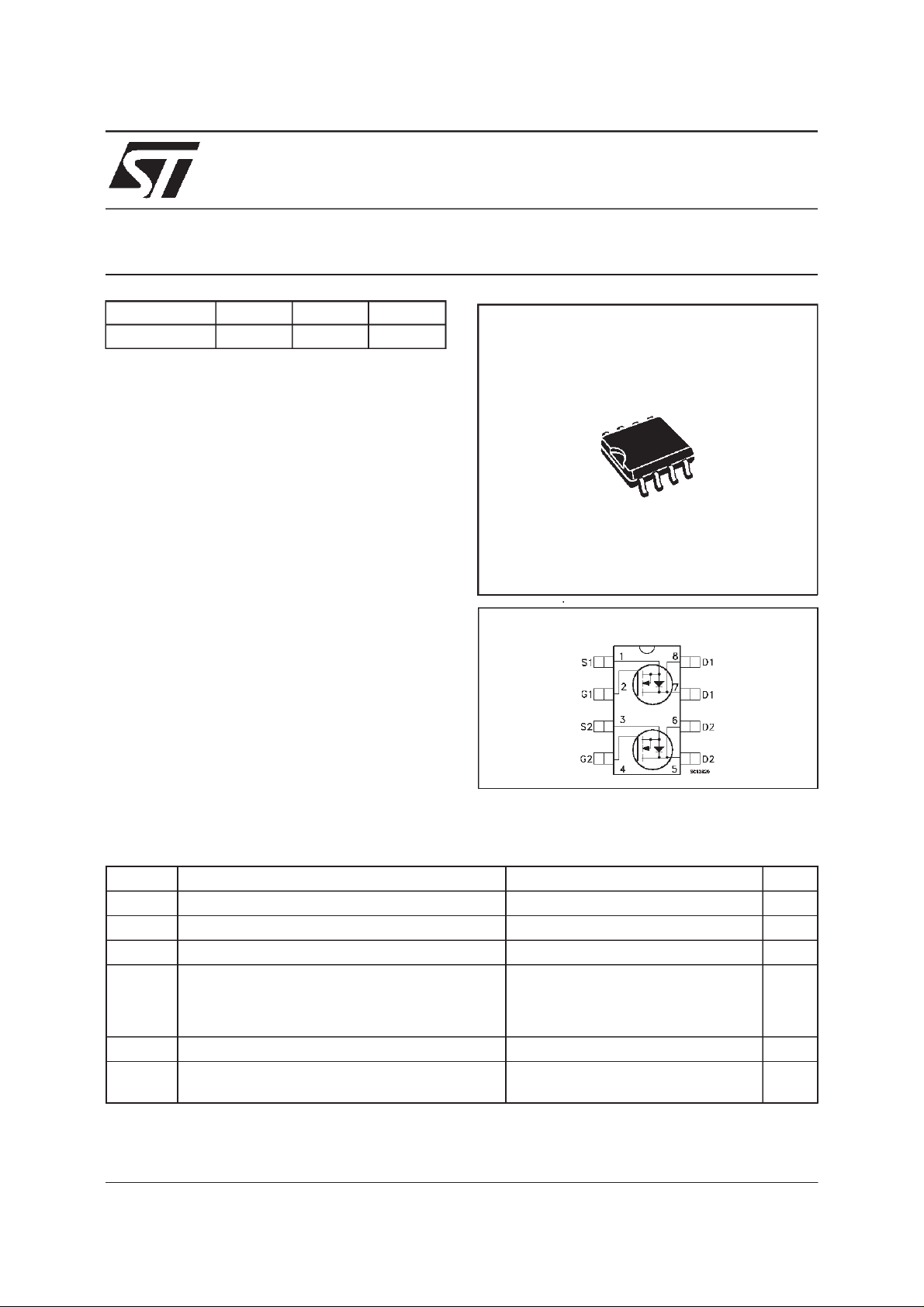
DUAL N - CHANNEL30V - 0.022Ω - 6A SO-8
STripFET POWER MOSFET
TYPE V
ST S6DNF30L 30 V < 0.025 Ω 6A
■ TYPICALR
■ STANDARD OUTLINE FOR EASY
DS(on)
DSS
= 0.022 Ω
R
DS(on)
I
D
AUTOMATEDSURFACEMOUNTASSEMBLY
■ LOW THRESHOLDDRIVE
DESCRIPTION
This Power MOSFET is the secondgeneration of
STMicroelectronics unique ” Single Feature
Size
”
strip-based process. The resulting
transistor shows extremely high packing density
for low on-resistance, rugged avalanche
characteristics and less critical alignment steps
therefore a remarkable manufacturing
reproducibility.
APPLICATIONS
■ DC MOTOR DRIVE
■ DC-DCCONVERTERS
■ BATTERYMANAGMENTIN NOMADIC
EQUIPMENT
■ POWERMANAGEMENTIN
PORTABLE/DESKTOPPC
s
SO-8
INTERNAL SCHEMATIC DIAGRAM
ABSOLUTE MAXIMUM RATINGS
Symb o l Parameter Value Unit
V
V
V
I
DM
P
(•) Pulse width limited by safeoperating area
April 1999
Drain-source Volt age (VGS=0) 30 V
DS
Drain- gate Voltage (RGS=20kΩ)30V
DGR
Gate-s ource Voltage ± 20 V
GS
Drain Current (co ntinuous) at Tc = 25oC
I
D
Single Operat ion
Drain Current (co ntinuous) at T
Single Operat ion
(•) Drain Current (puls ed) 24 A
Tot al Di ssipation at Tc=25oC Dual Opera tion
tot
Tot al Di ssipation at T
=25oCSinlgeOperation
c
=100oC
c
6
3.8
2
1.6
A
A
W
W
1/8
STS6DNF30L
THERMAL DATA
R
thj-amb
T
Tstg
(*)Mountedon FR-4 board (Steady State)
*Ther mal Resistan c e Junction-amb ient S ingle Opera ti on
Maximum Operating Ju nc t ion T emperat ure
j
Sto rage Temperature
Dual Operation
78
62.5
150
-65 to 150
o
C/W
o
C/W
o
o
C
C
ELECTRICAL CHARACTERISTICS
=25oC unless otherwisespecified)
(T
case
OFF
Symbol Parameter Test Conditions Min. Typ. Max. Unit
V
(BR)DSS
Drain-source
ID=250µAVGS=0 30 V
Break dow n Voltage
I
DSS
I
GSS
Zero Gate Voltage
Drain Cur rent ( V
GS
Gat e- bod y L eakage
Current (V
DS
=0)
=0)
V
=MaxRating
DS
=MaxRating Tc=125oC
V
DS
V
=± 20 V
GS
1
10
100 nA
±
ON (∗)
Symbol Parameter Test Conditions Min. Typ. Max. Unit
V
GS(th)
R
DS(on)
I
D(on)
Gate Threshold Voltage VDS=VGSID= 250 µA11.62.5V
Sta t ic Drain -s ource On
Resistance
VGS=10V ID=3A
=4.5V ID=3A
V
GS
On State Drain Current VDS>I
D(on)xRDS(on )max
0.022
0.025
6A
0.025
0.032ΩΩ
VGS=10V
DYNAMIC
Symbol Parameter Test Conditions Min. Typ. Max. Unit
g
(∗)Forward
fs
Tr ansc on duc tance
C
C
C
Input Capac i t ance
iss
Out put Capacitance
oss
Reverse Tr ansfer
rss
Capacit a nc e
VDS>I
D(on)xRDS(on )maxID
=3A 9 S
VDS=25V f=1MHz VGS= 0 V 1250
230
50
µA
µA
pF
pF
pF
2/8

STS6DNF30L
ELECTRICAL CHARACTERISTICS
(continued)
SWITCHINGON
Symbol Parameter Test Conditions Min. Typ. Max. Unit
t
d(on)
Tur n-on Delay Time
Rise Ti me
t
r
VDD=15V ID=3A
R
=4.7
G
Ω
VGS=4.5V
22
30
(Resis t iv e Loa d, see f ig. 3 )
Q
Q
Q
Tot al Gat e Charge
g
Gat e- Source Charg e
gs
Gate-Drain Charge
gd
VDD=24V ID=6A VGS=4.5V 17
4
6
23 nC
SWITCHINGOFF
Symbol Parameter Test Conditions Min. Typ. Max. Unit
t
d(off)
Tur n-of f Delay Time
t
Fall T ime
f
VDD=15V ID=3A
=4.7 Ω VGS=4.5V
R
G
55
10
(Resis t iv e Loa d, see f ig. 3 )
t
r(Voff)
t
t
Off-volt age Rise T im e
Fall T ime
f
Cross-over Time
c
V
=24V ID=6A
clamp
=4.7 Ω VGS=4.5V
R
G
(Indu ct iv e Load , s e e fig. 5)
10
18
30
SOURCEDRAINDIODE
Symbol Parameter Test Conditions Min. Typ. Max. Unit
I
V
I
SDM
SD
Q
I
RRM
SD
t
Source-drain Current
(•)
Source-drain Current
6
24
(pulsed)
(∗)ForwardOnVoltage ISD=6A VGS=0 1.2 V
Reverse Recovery
rr
Time
Reverse Recovery
rr
ISD=6A di/dt=100A/µs
=20V Tj=150oC
V
DD
(see test circuit, fig. 5)
30
30
Charge
Reverse Recovery
2
Current
ns
ns
nC
nC
ns
ns
ns
ns
ns
A
A
ns
nC
A
(∗) Pulsed: Pulse duration = 300 µs, duty cycle 1.5 %
(•) Pulse width limited by safe operatingarea
SafeOperating Area ThermalImpedance
3/8
 Loading...