

P - CHANNEL30V - 0.053Ω - 5A SO-8
TYPE V
ST S5P F30L 30 V < 0.060 Ω 5A
■ TYPICALR
■ STANDARD OUTLINE FOR EASY
DS(on)
DSS
= 0.053 Ω
AUTOMATEDSURFACEMOUNTASSEMBLY
■ LOW THRESHOLDDRIVE
DESCRIPTION
This Power MOSFET is the secondgeneration of
STMicroelectronicsunique ”Single Feature Size
”
strip-based process. The resulting transistor
shows extremely high packing density for low onresistance, rugged avalanche characteristics and
less critical alignment steps therefore a remarkable manufacturingreproducibility.
APPLICATIONS
■ BATTERYMANAGMENTIN NOMADIC
EQUIPMENT
■ POWERMANAGMENT IN CELLULAR
PHONES
R
DS(on)
I
D
STS5PF30L
STripFET POWER MOSFET
PRELIMINARY DATA
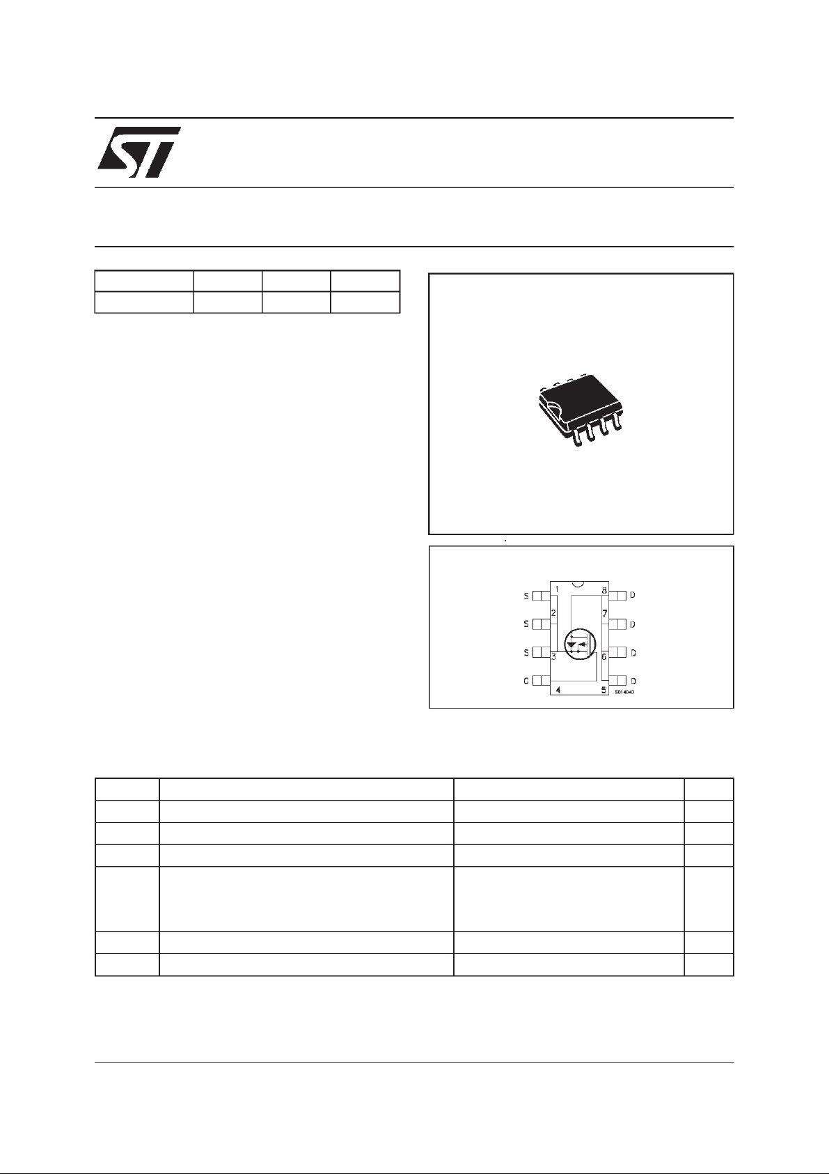
SO-8
INTERNAL SCHEMATIC DIAGRAM
ABSOLUTE MAXIMUM RATINGS
Symb o l Parameter Value Unit
V
V
V
I
DM
P
(•) Pulsewidth limited by safeoperating area
Note: For the P-CHANNEL MOSFET actual polarity of voltages and current has to be reversed
November 1999
Drain-source Voltage (VGS=0) 30 V
DS
Drain- gate V olt ag e (RGS=20kΩ)30V
DGR
Gate-s ource Voltage ± 20 V
GS
Drain C ur rent (co nt inuous) at Tc = 25oC
I
D
Single Operat ion
Drain C ur rent (co nt inuous) at T
Single Operat ion
(•) Drain C ur rent (pu lsed) 20 A
Tot al Dis sipation at Tc=25oC 2.5 W
tot
=100oC
c
5
3
A
A
1/6
STS5PF30L
THERMAL DATA
R
thj-amb
T
T
(*)
Mountedon FR-4board (t
*Ther mal Resistan c e Junction-amb ient
Maximum Operat ing Ju nct ion T emperat ure
j
Sto rage Temper at ure
stg
≤ 10
sec)
50
150
-55 to 150
o
C/W
o
C/W
o
C
ELECTRICAL CHARACTERISTICS (T
=25oC unless otherwisespecified)
case
OFF
Symbol Parameter Test Conditions Min. Typ. Max. Unit
V
(BR)DSS
Drain-source
ID=250µAVGS=0 30 V
Break dow n V o lt age
I
I
ON (∗
DSS
GSS
Zero Gate Voltage
Drain Curr e nt (V
Gat e- bod y L eakag e
Current (V
)
DS
=0)
GS
=0)
V
=MaxRating
DS
=MaxRating Tc=125oC
V
DS
V
= ± 20 V ± 100 nA
GS
1
10
Symbol Parameter Test Conditions Min. Typ. Max. Unit
V
GS(th)
R
DS(on)
I
D(on)
Gate Threshold Voltage VDS=VGSID= 250 µA11.62.5V
Sta t ic Drain -s our c e O n
Resistance
On State Drain Current VDS>I
VGS=10V ID=3A
V
=4.5V ID=3A
GS
D(on)xRDS(on )max
0.053
0.067
0.060
0.075
5A
VGS=10V
DYNAMIC
Symbol Parameter Test Conditions Min. Typ. Max. Unit
g
(∗)Forward
fs
Tr ansc on duc tance
C
C
C
Input Capacitance
iss
Out put Capacitance
oss
Reverse Tr ansfer
rss
Capacit a nc e
VDS>I
D(on)xRDS(on )maxID
=3A 10 S
VDS=25V f=1MHz VGS= 0 V 1350
490
130
µA
µ
Ω
Ω
pF
pF
pF
A
2/6

STS5PF30L
ELECTRICAL CHARACTERISTICS
(continued)
SWITCHINGON
Symbol Parameter Test Conditions Min. Typ. Max. Unit
t
d(on)
Tur n-on Delay Time
Rise Ti me
t
r
VDD=15V ID=2A
R
=4.7
G
Ω
VGS=4.5V
25
35
(Resis t iv e Loa d, s ee fig.3)
Q
Q
Q
Tot al Gat e Charge
g
Gat e- Source Charge
gs
Gate-Drain Charge
gd
VDD=24V ID=4A VGS= 5 V 12.5
5
3
16 nC
SWITCHINGOFF
Symbol Parameter Test Conditions Min. Typ. Max. Unit
t
d(off)
Tur n-of f Delay Time
t
Fall T ime
f
VDD=24V ID=2A
=4.7 Ω VGS=4.5V
R
G
125
35
(Resis t iv e Loa d, s ee fig.3)
SOURCEDRAINDIODE
Symbol Parameter Test Conditions Min. Typ. Max. Unit
I
SD
I
SDM
V
SD
t
Q
I
RRM
(∗) Pulsed: Pulse duration = 300 µs, duty cycle 1.5 %
(•) Pulse width limited by safe operatingarea
Source-drain Current
(•)
Source-drain Current
5
20
(pulsed)
(∗)ForwardOnVoltage ISD=5A VGS=0 1.2 V
Reverse Recovery
rr
Time
Reverse Recovery
rr
ISD= 5 A di/dt = 100 A/µs
=20V Tj= 150oC
V
r
(see test circuit, fig.5)
tbd
tbd
Charge
Reverse Recovery
tbd
Current
ns
ns
nC
nC
ns
ns
A
A
ns
nC
A
3/6

STS5PF30L
Fig. 1:
UnclampedInductiveLoad TestCircuit
Fig. 3: SwitchingTimes Test Circuits For
ResistiveLoad
Fig. 2:
UnclampedInductiveWaveform
Fig. 4: Gate Chargetest Circuit
Fig. 5:
Test CircuitFor InductiveLoad Switching
And Diode Recovery Times
4/6

SO-8 MECHANICALDATA
STS5PF30L
DIM.
MIN. TYP. MAX. MIN. TYP. MAX.
A 1.75 0.068
a1 0.1 0.25 0.003 0.009
a2 1.65 0.064
a3 0.65 0.85 0.025 0.033
b 0.35 0.48 0.013 0.018
b1 0.19 0.25 0.007 0.010
C 0.25 0.5 0.010 0.019
c1 45 (typ.)
D 4.8 5.0 0.188 0.196
E 5.8 6.2 0.228 0.244
e 1.27 0.050
e3 3.81 0.150
F 3.8 4.0 0.14 0.157
L 0.4 1.27 0.015 0.050
M 0.6 0.023
S 8 (max.)
mm inch
0016023
5/6

STS5PF30L
Information furnishedis believed to be accurateand reliable.However, STMicroelectronics assumes no responsibilityfor the consequences
of use of such information nor for any infringement of patents or other rights of third parties which may result from its use. No license is
granted by implication or otherwise under anypatent or patent rights of STMicroelectronics. Specificationmentioned in this publication are
subjecttochange withoutnotice.Thispublication supersedes and replaces all informationpreviously supplied. STMicroelectronicsproducts
are not authorized for use as critical components in lifesupport devices or systemswithout express written approval of STMicroelectronics.
The STlogo is a trademark of STMicroelectronics
1999 STMicroelectronics – Printed in Italy – All Rights Reserved
STMicroelectronics GROUP OF COMPANIES
Australia - Brazil - China - Finland - France - Germany - Hong Kong - India - Italy - Japan- Malaysia - Malta - Morocco -
6/6
Singapore - Spain - Sweden - Switzerland - United Kingdom - U.S.A.
http://www.st.com
.
 Loading...