

STripFET™ MOSFET PLUS SCHOTTKY RECTIFIER
MAIN PRODUCT CHARACTERISTICS
MOSFET
V
DSS
20 V < 0.07
R
DS(on)
STS4DPFS2LS
P-CHANNEL 20V - 0.06Ω - 4A SO-8
I
D
Ω
4 A
SCHOTTKY
I
F(AV )
3 A 40 V 0.44 V
V
RRM
V
F(MAX)
SO-8
DESCRIPTION
This product associates the latest low voltage
STripFET™ in p-channel version to a low drop
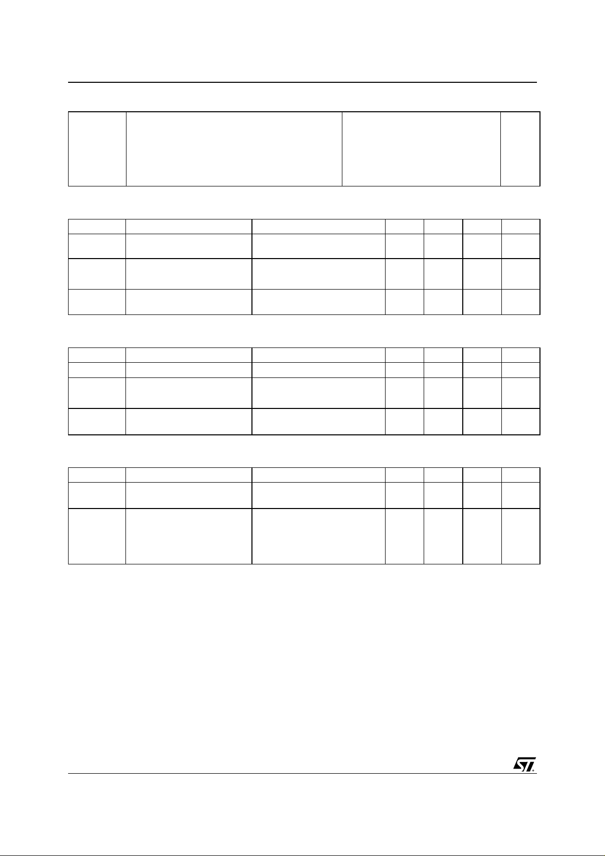
INTERNAL SCHEMATIC DIAGRAM
Schottky diode. Such configuration is extremely versatile in implementing, a large variety of DC-DC
converters for printers, portable equipment, and cellular phones.
MOSFET ABSOLUTE MAXIMUM RATINGS
Symbol Parameter Value Unit
V
DS
V
DGR
V
GS
I
D
I
D
I
(●)
DM
P
TOT
E
AS
Drain-source Voltage (VGS = 0)
Drain-gate Voltage (RGS = 20 kΩ)
20 V
20 V
Gate- source Voltage ± 20 V
Drain Current (continuos) at TC = 25°C
Drain Current (continuos) at TC = 100°C
4A
3.4 A
Drain Current (pulsed) 16 A
Total Dissipation at TC = 25°C
(1)
Single Pulse Avalanche Energy 20 mJ
2W
SCHOTTKY ABSOLUTE MAXIMUM RATINGS
Symbol Parameter Value Unit
V
RRM
I
F(RMS)
I
F(AV)
I
FSM
I
RRM
dv/dt
(•)Pu l se width limite d by safe operat i ng area
(1) Starting T
Repetitive Peak Reverse Voltage 40 V
RMS Forward Current 10 A
Average Forward Current TL = 120°C
δ
= 0.5
Surge Non Repetitive Forward Current tp = 10 ms
3A
75 A
Sinusoidal
Repetitive Peak Reverse Current tp = 2 µs
1A
F = 1 kHz
Critical Rate Of Rise Of Reverse Voltage 10000 V/µs
= 25°C, ID = 2.5 A, VDD = 20 V
j
Note: For the P-CHANNEL MOSFET actual polarity of Voltages
and current has to be reversed
1/8February 2001
STS4DPFS2LS
THERMA L D ATA
Rthj-amb (*)Thermal Resistance Junction-ambient MOSFET 62.5 °C/W
Rthj-amb (*)Thermal Resistance Junction-ambient SCHOTTKY 100 °C/W
T
stg
T
l
MOSFET ELECTRICAL CHARACTERISTICS (TCASE = 25 °C UNLESS OTHERWISE SPECIFIED)
OFF
Symbol Parameter Test Conditions Min. Typ. Max. Unit
V
(BR)DSS
I
DSS
I
GSS
ON (1)
Symbol Parameter Test Conditions Min. Typ. Max. Unit
V
GS(th)
R
DS(on)
I
D(on)
Storage Temperature Range -55 to 150 °C
Junction Temperature 150 °C
(*) Mounted on FR-4 board (Steady State)
Drain-source
ID = 250 µA, VGS = 0 20 V
Breakdown Voltage
Zero Gate Voltage
Drain Current (V
GS
= 0)
Gate-body Leakage
Current (V
DS
= 0)
Gate Threshold Voltage
Static Drain-source On
Resistance
On State Drain Current VDS > I
V
= Max Rating
DS
V
= Max Rating, TC = 125 °C
DS
V
= ± 20 V ±100 nA
GS
V
= VGS, ID = 250µA
DS
VGS = 10V, ID = 2.5 A
VGS = 4.5V, ID = 2.5 A
x R
D(on)
DS(on)max,
1 1.6 2.5 V
0.06 0.07
0.07 0.085
16 A
1µA
10 µA
VGS=10V
Ω
DYNAMIC
Symbol Parameter Test Conditions Min. Typ. Max. Unit
(1) Forward Transconductance VDS > I
g
fs
C
iss
C
oss
C
rss
Input Capacitance
Output Capacitance 490 pF
Reverse Transfer
Capacitance
ID=2 A
V
DS
x R
D(on)
DS(on)max,
= 25V, f = 1 MHz, VGS = 0
5S
1350 pF
130 pF
2/8
STS4DPFS2LS
ELECTRICAL CHARACTERISTICS (CONTINUED)
SWITCHING ON
Symbol Parameter Test Conditions Min. Typ. Max. Unit
V
t
d(on)
Q
Q
Q
t
r
gs
gd
Turn-on Delay Time
Rise Time 35 ns
Total Gate Charge
g
Gate-Source Charge 5 nC
Gate-Drain Charge 3 nC
SWITCHING OFF
Symbol Parameter Test Conditions Min. Typ. Max. Unit
t
d(off)
t
t
r(Voff)
t
t
f
f
c
Turn-off Delay Time
Fall Time
Off-voltage Rise Time
Fall Time
Cross-over Time
SOURCE DRAIN DIODE
Symbol Parameter Test Conditions Min. Typ. Max. Unit
I
SD
I
SDM
VSD (1)
t
rr
Q
rr
I
RRM
Note: 1. Pulsed: Pu l se duration = 300 µs, duty cycl e 1. 5 %.
2. Pulse width li mited by safe operating area.
Source-drain Current 4 A
(2)
Source-drain Current (pulsed) 16 A
Forward On Voltage
Reverse Recovery Time
Reverse Recovery Charge 36 nC
Reverse Recovery Current 1.6 A
= 15V, ID = 3A RG=4.7Ω
DD
V
= 10V
GS
(see test circuit, Figure 3)
V
= 24V, ID = 6A,
DD
VGS = 4.5 V
VDD = 15 V, ID = 2A,
RG=4.7Ω, V
GS
= 4.5 V
(see test circuit, Figure 3)
= 24 V, ID = 6 A,
V
clamp
RG=4.7Ω, V
GS
= 4.5 V
(see test circuit, Figure 5)
ISD = 4 A, VGS = 0
I
= 4 A, di/dt = 100A/µs,
SD
V
= 15 V, Tj = 150°C
DD
(see test circuit, Figure 5)
25 ns
12.5 16 nC
125
30
83
40
75
1.2 V
45 ns
ns
ns
ns
ns
ns
SCHOTTCKY STATIC ELETTRICAL CHARACTERISTICS
Symbol Parameter Test Conditions Min. Typ. Max. Unit
(*) Reve rsed Leak age Curren t TJ = 25 °C , VR = 30 V
I
R
TJ = 125 °C , VR = 30 V
(*) Forward Voltage Drop TJ = 25 °C , IF = 1 A
V
F
T
= 125 °C , IF = 1 A
J
TJ = 25 °C , IF = 2 A
TJ = 125 °C , IF = 2 A
TJ = 25 °C , IF = 3 A
T
= 125 °C , IF = 3 A
J
14
8
0.37
0.28
0.41
0.34
0.4
50
18
0.42
0.32
0.46
0.39
0.5
0.44
µ
mA
V
V
V
V
V
V
A
3/8

STS4DPFS2LS
Safe Operating Area Thermal Impedance
Output Characteristics
Transfer Characteristics
Static Drain-source On ResistanceTransconductance
4/8

STS4DPFS2LS
Capacitance VariationsGate Charge vs Gate-source Voltage
Normalized Gate Threshold Volta ge vs Temp. Normalized On Resistance vs Temperatur e
Source-drain Diode Forward Characteristics
5/8

STS4DPFS2LS
Fig. 2: Unclamped Inductive WaveformFig. 1: Unclamped Inductive Load Test Circuit
Fig. 3: Switching Times Test Circuits For
Resistive Load
Fig. 5: Test Circuit For Inductive Load Switching
And Diode Recovery Times
Fig. 4: Gate Charge test Circuit
6/8

SO-8 MECHANICAL DATA
STS4DPFS2LS
DIM.
MIN. TYP. MAX. MIN. TYP. MAX.
A1.750.068
a1 0.1 0.25 0.003 0.009
a2 1.65 0.064
a3 0.65 0.85 0.025 0.033
b 0.35 0.48 0.013 0.018
b1 0.19 0.25 0.007 0.010
C 0.25 0.5 0.010 0.019
c1 45 (typ.)
D 4.8 5.0 0.188 0.196
E 5.8 6.2 0.228 0.244
e1.27 0.050
e3 3.81 0.150
F 3.8 4.0 0.14 0.157
L 0.4 1.27 0.015 0.050
M0.60.023
S 8 (max.)
mm inch
0016023
7/8

STS4DPFS2LS
8/8
Information furnished is believed to be accurate and reliable. However, STMicroelectronics assumes no responsibility for the consequences
of use of such informa tion n or for an y infring ement of patent s or other rig hts of third part ies which may resu lt from its use . No l i cen se i s
granted by implication or otherwise under any patent or patent rights of STMicroelectronics. Specification mentioned in this publication are
subject to change without notice. This publication supersedes and replaces all information previously supplied. STMicroelectronics products
are not authorized for use as critical compo nents in life support devices or systems without express written approval of STMicroelectronics.
Australia - Brazil - China - Finland - France - Germany - Hong Kong - India - Italy - Japan - Malaysia - Malta - Morocco -
The ST logo is a trademark of STMicroelectronics
© 2000 STMicroelectronics – Printed in Italy – All Rights Reserved
STMicroelectronics GROUP OF COMPANIES
Singapore - Spain - Sweden - Switzerland - United Kingdom - U.S.A.
http://www.st.com
 Loading...