

SGS Thomson Microelectronics STS4DPF30L Datasheet
STS4DPF30L
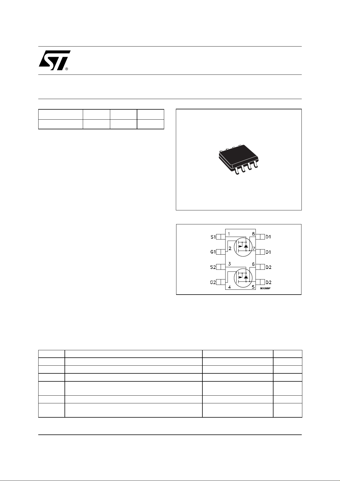
DUAL P-CHANNEL 30V - 0.07 Ω - 4A SO-8
STripFET™ POWER MOSFET
PRELIMINARY DATA
TYPE
V
DSS
STS4DPF30L 30 V <0.08
■ TYPICAL R
■ STANDARD OUTLINE FO R EAS Y
(on) = 0.07 Ω
DS
R
DS(on)
I
D
Ω
4 A
AUTOMATED SURFACE MOUNT ASSEMBLY
■ LOW THRESHOLD DRIVE
DESCRIPTION
This Power MOSFET is the latest dev elo pment of
STMicroelectronis unique "Single Feature Size™"
strip-based process. The resulting transistor
shows extremely high packing density for low onresistance, rugged avalanche characteristics and
less critical alignment steps therefore a remarkable manufacturing reproducibility.
APPLICATIONS
■ BATTERY MANAGEMENT IN NOMADIC
EQUIPMENT
■ POWER MANAGEMENT IN CELLULAR
PHONES
■ DC-DC CONVERTER
SO-8
INTERNAL SCHEMATIC DIAGRAM
ABSOLUTE MAXIMUM RATINGS
Symbol Parameter Value Unit
V
V
DGR
V
I
I
DM
P
(
Puls e width limit ed by safe opera ti ng are a. Note: F or t he P- CHA NNE L MOS FE T ac tu al po la rity o f v olt ages a nd
•)
April 2002
This is preliminary information on a new product now in development or undergoing evaluation. Details are subject to change without notice.
Drain-source Voltage (VGS = 0)
DS
Drain-gate Voltage (RGS = 20 kΩ)
Gate- source Voltage ± 16 V
GS
Drain Current (continuous) at TC = 25°C Single Operation
D
Drain Current (continuous) at T
(
•)
Drain Current (pulsed) 16 A
Total Dissipation at TC = 25°C Dual Operation
tot
Total Dissipation at T
= 25°C Single Operation
C
= 100°C Single Operation
C
current has to be rever sed
30 V
30 V
4
2.5
2.0
1.6
A
A
W
W
1/6
STS4DPF30L
THERMAL DATA
Rthj-amb
T
T
stg
(*)
When Mounted on 1 inch2 FR-4 board, 2 oz of Cu and t [ 10 sec.
(*)Thermal Resistance Junction-ambient Single Operation
Thermal Operating Junction-ambient
j
Storage Temperature
Dual Operating
78
62.5
-55 to150
-55 to 150
°C/W
°C/W
°C
°C
ELECTRICAL CHARACTERISTICS (T
= 25 °C UNLESS OTHERWISE SPECIFIED)
CASE
OFF
Symbol Parameter Test Conditions Min. Typ. Max. Unit
I
V
(BR)DSS
Drain-source
= 250 µA, VGS = 0
D
30 V
Breakdown Voltage
V
= Max Rating
DS
V
= Max Rating TC = 125°C
DS
V
= ± 16 V
GS
1
10
±100 nA
ON
(*)
I
DSS
I
GSS
Zero Gate Voltage
Drain Current (V
GS
Gate-body Leakage
Current (V
DS
= 0)
= 0)
Symbol Parameter Test Conditions Min. Typ. Max. Unit
V
V
GS(th)
R
DS(on)
Gate Threshold Voltage
Static Drain-source On
Resistance
= VGS I
DS
= 10 V ID = 2 A
V
GS
V
= 4.5 V ID = 2 A
GS
= 250 µA
D
1V
0.070
0.085
0.08
0.10
DYNAMIC
Symbol Parameter Test Conditions Min. Typ. Max. Unit
(*)
g
fs
C
iss
C
oss
C
rss
Forward Transconductance
Input Capacitance
Output Capacitance
Reverse Transfer
Capacitance
V
= 15V ID=2 A
DS
= 25V, f = 1 MHz, VGS = 0
V
DS
10 S
1350
490
130
µA
µA
Ω
Ω
pF
pF
pF
2/6
 Loading...