

STS4DPF20L
DUAL P-CHANNEL 20V - 0.07 Ω - 4A SO-8
STripFET™ POWER MOSFET
TYPE
STS4DPF20L 20 V <0.08
■ TYPICAL R
■ STANDARD OUTLINE FO R EAS Y
V
DSS
(on) = 0.07 Ω
DS
R
DS(on)
I
D
Ω
4 A
AUTOMATED SURFACE MOUNT ASSEMBLY
■ LOW THRESHOLD DRIVE
DESCRIPTION
This Power MOSFET is the latest dev elo pment of
STMicroelectronis unique "Single Feature Size™"
strip-based process. The resulting transistor
shows extremely high packing density for low onresistance, rugged avalanche characteristics and
less critical alignment steps therefore a remarkable manufacturing reproducibility.
APPLICATIONS
■ BATTERY MANAGEMENT IN NOMADIC
EQUIPMENT
■ POWER MANAGEMENT IN CELLULAR
PHONES
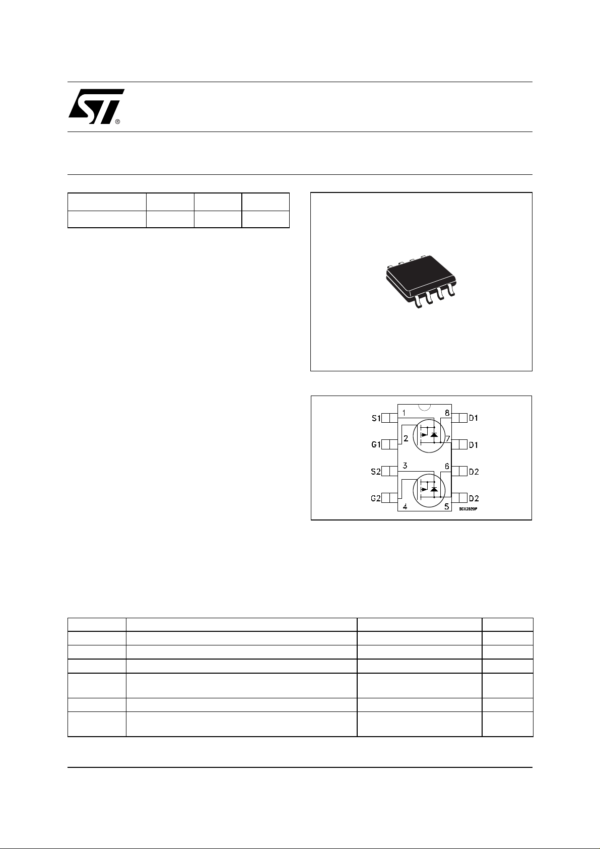
SO-8
INTERNAL SCHEMATIC DIAGRAM
ABSOLUTE MAXIMUM RATINGS
Symbol Parameter Value Unit
V
DS
V
DGR
V
GS
I
D
(
I
DM
P
tot
(
Puls e width limit ed by safe opera ti ng are a. Note: F or t he P- CHA NNE L MOS FE T ac tu al po la rity o f v olt ages a nd
•)
.
Drain-source Voltage (VGS = 0)
Drain-gate Voltage (RGS = 20 kΩ)
Gate- source Voltage ± 16 V
Drain Current (continuos) at TC = 25°C Single Operation
Drain Current (continuos) at T
•)
Drain Current (pulsed) 16 A
Total Dissipation at TC = 25°C Dual Operation
Total Dissipation at T
= 25°C Single Operation
C
= 100°C Single Operation
C
current has to be rever sed
20 V
20 V
4
2.5
1.6
2
A
A
W
W
1/8February 2002
STS4DPF20L
THERMAL DATA
Rthj-amb
T
T
stg
(*)
When Mounted on 0.5 in2 pad of 2 oz.cop per
(*)Thermal Resistance Junction-ambient Single Operation
Thermal Operating Junction-ambient
j
Storage Temperature
Dual Operating
62.5
78
-55 to150
-55 to 150
°C/W
°C/W
°C
°C
ELECTRICAL CHARACTERISTICS (T
= 25 °C UNLESS OTHERWISE SPECIFIED)
CASE
OFF
Symbol Parameter Test Conditions Min. Typ. Max. Unit
I
V
(BR)DSS
Drain-source
= 250 µA, VGS = 0
D
20 V
Breakdown Voltage
= Max Rating
V
DS
V
= Max Rating TC = 125°C
DS
V
= ± 16 V
GS
1
10
±100 nA
ON
(*)
I
DSS
I
GSS
Zero Gate Voltage
Drain Current (V
GS
Gate-body Leakage
Current (V
DS
= 0)
= 0)
Symbol Parameter Test Conditions Min. Typ. Max. Unit
V
V
GS(th)
R
DS(on)
Gate Threshold Voltage
Static Drain-source On
Resistance
= VGS I
DS
= 10 V ID = 2 A
V
GS
V
= 4.5 V ID = 2 A
GS
= 250 µA
D
1 1.6 2.5 V
0.070
0.085
0.08
0.10
DYNAMIC
Symbol Parameter Test Conditions Min. Typ. Max. Unit
(*)
g
fs
C
iss
C
oss
C
rss
Forward Transconductance
Input Capacitance
Output Capacitance
Reverse Transfer
Capacitance
V
= 15V ID=2 A
DS
= 25V, f = 1 MHz, VGS = 0
V
DS
10 S
1350
490
130
µA
µA
Ω
Ω
pF
pF
pF
2/8
STS4DPF20L
ELECTRICAL CHARACTERISTICS (continued)
SWITCHING ON
Symbol Parameter Test Conditions Min. Typ. Max. Unit
= 15 V ID = 2 A
t
d(on)
Turn-on Delay Time
t
r
Rise Time
V
DD
R
= 4.7 Ω VGS = 4.5 V
G
(Resistive Load, Figure 1)
Q
g
Q
gs
Q
gd
Total Gate Charge
Gate-Source Charge
Gate-Drain Charge
= 24V ID= 4A VGS=5V
V
DD
(See test circuit, Figure 2)
SWITCHING OFF
Symbol Parameter Test Conditions Min. Typ. Max. Unit
= 15 V ID = 2 A
t
d(off)
Turn-off Delay Time
t
f
Fall Time
V
DD
R
= 4.7Ω, V
G
GS
= 4.5 V
(Resistive Load, Figure 1)
SOURCE DRAIN DIODE
Symbol Parameter Test Conditions Min. Typ. Max. Unit
I
SD
I
SDM
V
SD
t
rr
Q
rr
I
RRM
(*)
Pulsed: P ul se duration = 300 µs, duty cycle 1.5 %.
(
•)Pulse width limited by s afe operating area.
Source-drain Current
(•)
Source-drain Current (pulsed)
(*)
Forward On Voltage
Reverse Recovery Time
Reverse Recovery Charge
Reverse Recovery Current
I
= 4 A VGS = 0
SD
= 4 A di/dt = 100A/µs
I
SD
V
= 15 V Tj = 150°C
DD
(See test circuit, Figure 3)
25
35
12.5
5
3
125
35
45
36
1.6
16 nC
4
16
1.2 V
ns
ns
nC
nC
ns
ns
A
A
ns
nC
A
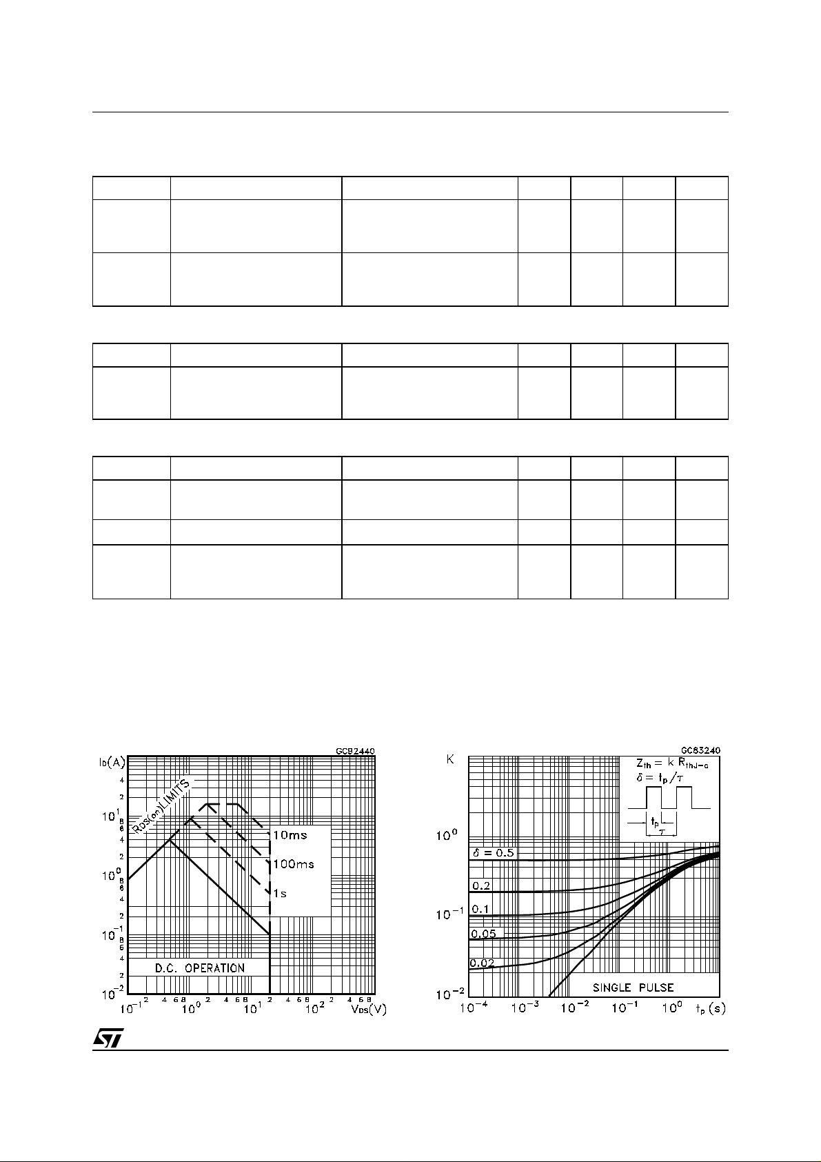
Safe Operating Area
Thermal Impedance
3/8

STS4DPF20L
Output Characteristics Transfer Characteristics
Transconductance Static Drain-source On Resistance
Gate Charge vs Gate-source Voltage Capacitance Variations
4/8

STS4DPF20L
Normalized Gate Threshold Voltage vs Temperature Normalized on Resistance vs Temperature
Source-drain Diode Forward Characteristics .
. .
5/8

STS4DPF20L
Fig. 1: Switching Times Test Circuits For Resistive
Load
Fig. 3: Test Circuit For Diode Recovery Behaviour
Fig. 2: Gate Charge test Circuit
6/8

SO-8 MECHANICAL DATA
STS4DPF20L
DIM.
MIN. TYP. MAX. MIN. TYP. MAX.
A1.750.068
a1 0.1 0.25 0.003 0.009
a2 1.65 0.064
a3 0.65 0.85 0.025 0.033
b 0.35 0.48 0.013 0.018
b1 0.19 0.25 0.007 0.010
C 0.25 0.5 0.010 0.019
c1 45 (typ.)
D 4.8 5.0 0.188 0.196
E 5.8 6.2 0.228 0.244
e1.27 0.050
e3 3.81 0.150
F 3.8 4.0 0.14 0.157
L 0.4 1.27 0.015 0.050
M0.60.023
S 8 (max.)
mm inch
0016023
7/8

STS4DPF20L
Information furnished is believed to be accurate an d rel i able. However, STMicroelectro ni cs assumes no responsibility for the consequen ces
of use of such information nor for any infringement of patents or other rights of third parties which may result from its use. No license is granted
by implic ation or otherwise under any patent or patent ri ghts of STM i croelectr onics. Sp ecifications mentioned in thi s publication are subject
to change without notice. This publication supersedes and replaces all information previously supplied. STMicroelectronics product s are not
authorized for use as cri tical comp onents in lif e support devi ces or systems without express written approv al of STMicroel ectronics.
The ST log o i s registered trademark of STMicroelectronics
2002 STMi croelectronics - All Ri ghts Rese rved
All other names are the property of their respective ow ners.
Australi a - Brazil - Canada - China - Finland - France - Germ any - Hong Kong - India - Israel - Ital y - Japan - Malay sia - Malta - Morocco -
Singapor e - S pai n - Sweden - S witzerland - United Kingdom - United States.
STMicroelect ro n ics GRO UP OF COMPANI ES
http://www.st.com
8/8
 Loading...