

SGS Thomson Microelectronics STS3DPF20V Datasheet

STS3DPF20V
DUAL P-CHANNEL 20V - 0.090 Ω - 3A SO-8
STripFET™ POWER MOSFET
TYPE
V
DSS
STS3DPF20L 20 V <0.11
■ TYPICAL R
■ TYPICAL R
■ STANDARD OUTLIN E FO R EASY
(on) = 0.090 Ω @ 4.5 V
DS
(on) = 0.1 Ω @ 2.7 V
DS
R
DS(on)
I
D
Ω
3 A
AUTOMATED SURFACE MOUNT ASSEMBLY
■ ULTRA LOW THRESHOLD
GATE DRIVE (2.7 V)
DESCRIPTION
This Power MOSFET is the latest dev elo pment of
STMicroelectronis unique "Single Feature Size™"
strip-based process. The resulting transistor
shows extremely high packing density for low onresistance, rugged avalanche characteristics and
less critical alignment steps therefore a remarkable manufacturing reproducibility.
APPLICATIONS
■ BATTERY MANAGEMENT IN NOMADIC
EQUIPMENT
■ MOBILE PHONE APPLICATIONS
SO-8
INTERNAL SCHEMATIC DIAGRAM
ABSOLUTE MAXIMUM RATINGS
Symbol Parameter Value Unit
V
DS
V
DGR
V
GS
I
D
I
DM
P
tot
(
Puls e width limit ed by safe opera ti ng are a. Note: F or t he P- CHA NNE L MOS FE T ac tu al po la rity o f v olt ages a nd
•)
.
Drain-source Voltage (VGS = 0)
Drain-gate Voltage (RGS = 20 kΩ)
20 V
20 V
Gate- source Voltage ± 12 V
Drain Current (continuous) at TC = 25°C Single Operation
Drain Current (continuous) at T
(
•)
Drain Current (pulsed) 12 A
= 100°C Single Operation
C
Total Dissipation at TC = 25°C Dual Operation
Total Dissipation at T
= 25°C Single Operation
C
current has to be rever sed
3
1.9
1.6
2
A
A
W
W
1/8June 2002
STS3DPF20V
THERMAL DATA
Rthj-amb
T
T
stg
(*)
When Mounted on 0.5 in2 pad of 2 oz.cop per
(*)Thermal Resistance Junction-ambient Single Operation
Thermal Operating Junction-ambient
j
Storage Temperature
Dual Operating
62.5
78
-55 to150
-55 to 150
°C/W
°C/W
°C
°C
ELECTRICAL CHARACTERISTICS (T
= 25 °C UNLESS OTHERWISE SPECIFIED)
CASE
OFF
Symbol Parameter Test Conditions Min. Typ. Max. Unit
I
V
(BR)DSS
Drain-source
= 250 µA, VGS = 0
D
20 V
Breakdown Voltage
= Max Rating
V
DS
V
= Max Rating TC = 125°C
DS
V
= ± 12 V
GS
1
10
±100 nA
ON
(*)
I
DSS
I
GSS
Zero Gate Voltage
Drain Current (V
GS
Gate-body Leakage
Current (V
DS
= 0)
= 0)
Symbol Parameter Test Conditions Min. Typ. Max. Unit
V
V
GS(th)
R
DS(on)
Gate Threshold Voltage
Static Drain-source On
Resistance
= VGS ID = 250 µA
DS
= 4.5 V ID = 1.5 A
V
GS
V
= 2.7 V ID = 1.5 A
GS
0.6 V
0.090
0.100
0.110
0.135
DYNAMIC
Symbol Parameter Test Conditions Min. Typ. Max. Unit
(*)
g
fs
C
iss
C
oss
C
rss
Forward Transconductance
Input Capacitance
Output Capacitance
Reverse Transfer
Capacitance
V
= 15 V ID=2 A
DS
= 25V, f = 1 MHz, VGS = 0
V
DS
7.5 S
500
140
30
µA
µA
Ω
Ω
pF
pF
pF
2/8
STS3DPF20V
ELECTRICAL CHARACTERISTICS (continued)
SWITCHING ON
Symbol Parameter Test Conditions Min. Typ. Max. Unit
= 10 V ID = 1.5 A
t
d(on)
Turn-on Delay Time
t
r
Rise Time
V
DD
R
= 4.7 Ω VGS = 4.5 V
G
(Resistive Load, Figure 1)
Q
Q
gs
Q
gd
Total Gate Charge
g
Gate-Source Charge
Gate-Drain Charge
= 10V ID= 3A VGS=5V
V
DD
(See test circuit, Figure 2)
SWITCHING OFF
Symbol Parameter Test Conditions Min. Typ. Max. Unit
= 10 V ID = 1.5 A
t
d(off)
Turn-off Delay Time
t
f
Fall Time
V
DD
R
= 4.7Ω, V
G
GS
= 4.5 V
(Resistive Load, Figure 1)
SOURCE DRAIN DIODE
Symbol Parameter Test Conditions Min. Typ. Max. Unit
I
SD
I
SDM
V
SD
t
rr
Q
rr
I
RRM
(*)
Pulsed: P ul se duration = 300 µs, duty cycle 1.5 %.
(
•)Pulse width limited by s afe operating area.
Source-drain Current
(•)
Source-drain Current (pulsed)
(*)
Forward On Voltage
Reverse Recovery Time
Reverse Recovery Charge
Reverse Recovery Current
I
= 3 A VGS = 0
SD
= 3 A di/dt = 100A/µs
I
SD
V
= 15 V Tj = 150°C
DD
(See test circuit, Figure 3)
38
39
6.2
1
1.4
54
12
20
13
1.3
8.5 nC
3
12
1.2 V
ns
ns
nC
nC
ns
ns
A
A
ns
nC
A
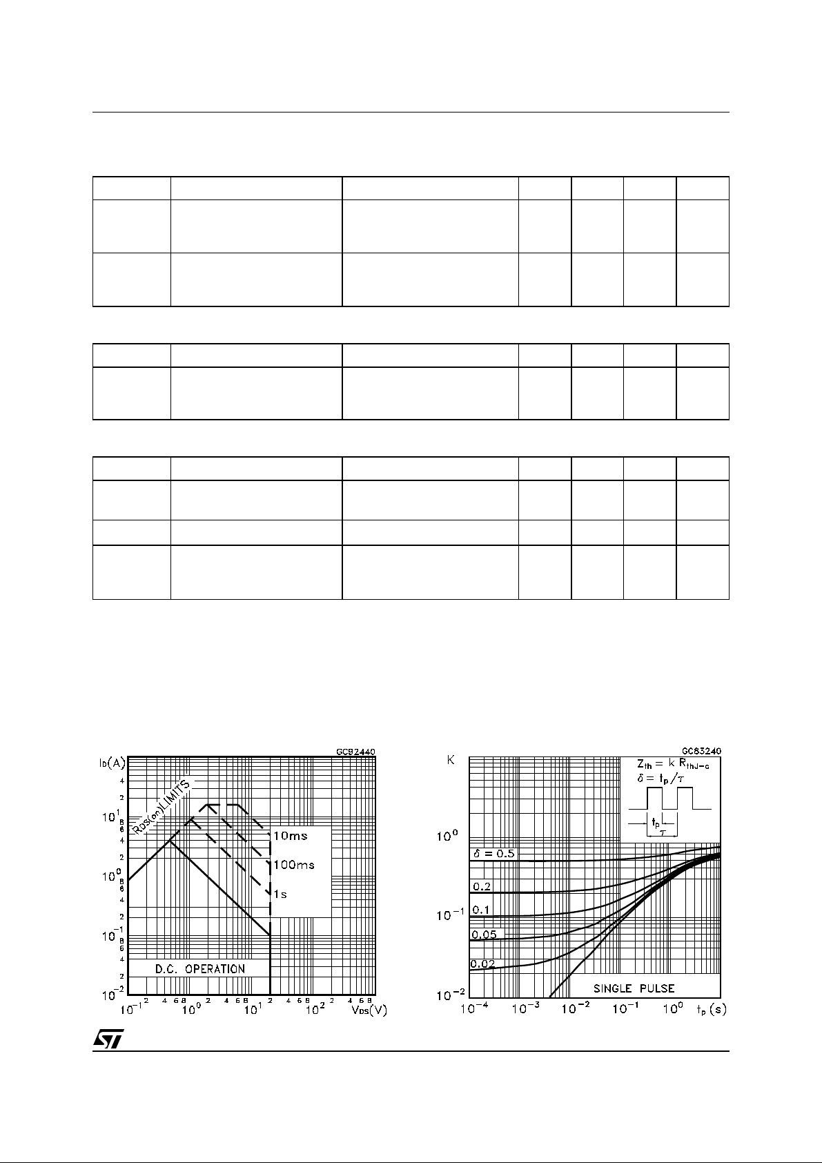
Safe Operating Area
Thermal Impedance
3/8
 Loading...