


TYPE
STS3C3F30L(N-Channel)
STS3C3F30L(P-Channel)
■ TYPICAL R
■ TYPICAL R
■ STANDARD OUTLI NE FO R EASY
(on) (N-Channel) = 50 mΩ
DS
(on) (P-Channel) = 140 mΩ
DS
V
30 V
30 V
DSS
R
DS(on)
< 65 m
< 165 m
Ω
Ω
AUTOMATED SURFACE MOUNT ASSEMBLY
■ LOW THRESHOLD DRIVE
STS3C3F30L
N-CHANNEL 30V - 0.050 Ω - 3.5A SO-8
P-CHANNEL 30V - 0.140 Ω - 3A SO-8
STripFET™ II POWER MOSFET
I
D
3.5 A
3 A
DESCRIPTION
SO-8
This application speci fic Power MOSFET is the second
generation of STMicro electronis unique "Single Feature
Size™" strip-based process. The resulting transistor
shows ext remely high packing densi ty for low on-resistance, rugge d avalan che cha racteristics and less criti cal
alignment steps therefore a remarkable manufacturing re-
INTERNAL SCHEMATIC DIAGRAM
producibility.
APPLICATIONS
■ DC/DC CONVERTERS
■ BATTERY MANAGEMENT IN NOMADIC
EQUIPMENT
■ POWER MANAGEMENT IN CELLULAR
PHONES
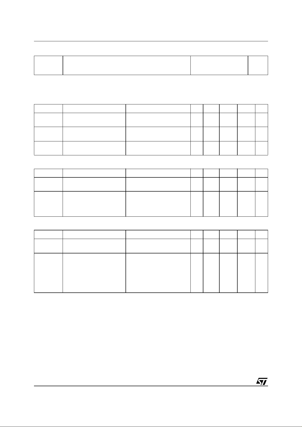
ABSOLUTE MAXIMUM RATINGS
Symbol Parameter N-CHANNEL P-CHANNEL Unit
V
DS
V
DGR
V
GS
I
D
I
D
I
(
DM
P
tot
T
stg
T
j
(
Pulse width limited by safe operating area. Note: P-CHANNEL MOSFET actual polarity of voltages and current
•)
.
Drain-source Voltage (VGS = 0)
Drain-gate Voltage (RGS = 20 kΩ)
30 V
30 V
Gate- source Voltage ± 16 V
Drain Current (continuos) at TC = 25°C
Single Operating
Drain Current (continuos) at TC = 100°C
Single Operating
•)
Drain Current (pulsed) 14 11 A
Total Dissipation at TC = 25°C Dual Operating
Total Dissipation at T
= 25°C Single Operating
C
3.5 2.7 A
2.2 1.7 A
1.6
2
Storage Temperature -60 to 150 °C
Max. Operating Junction Temperature 150 °C
has to be reversed
W
W
1/10February 2002
STS3C3F30L
THERMA L D ATA
Rthj-amb(1)
T
Thermal Resistance Junction-ambient Single Operation
Maximum Lead Temperature For Soldering Purpose
l
Dual Operating
62.5
78
300
°C/W
°C/W
°C
(1) when mounted on 0.5 in
ELECTRICAL CHARACTERISTICS (T
2
pad of 2 oz. copper
= 25 °C unless otherwise specified)
case
OFF
Symbol Parameter Test Conditions Min. Typ. Max. Unit
I
V
(BR)DSS
Drain-source
= 250 µA, VGS = 0
D
30
Breakdown Voltage
V
I
DSS
I
GSS
Zero Gate Voltage
Drain Current (V
GS
Gate-body Leakage
Current (V
DS
= 0)
= 0)
= Max Rating
DS
V
= Max Rating TC = 125°C
DS
= ± 16 V
V
GS
1
10
±100 nA
ON
Symbol Parameter Test Conditions Min. Typ. Max. Unit
V
V
GS(th)
R
DS(on)
Gate Threshold Voltage
Static Drain-source On
Resistance
= VGS I
DS
= 10 V ID = 1.75 A
V
GS
V
= 10 V ID = 1.5 A
GS
V
= 4.5 V ID = 1.75 A
GS
V
= 4.5 V ID = 1.5 A
GS
= 250 µA
D
n-ch
p-ch11
n-ch
p-ch
n-ch
p-ch
50
140
60
160
65
165
90
200
m
m
m
m
V
µA
µA
V
V
Ω
Ω
Ω
Ω
DYNAMIC
Symbol Parameter Test Conditions Min. Typ. Max. Unit
(*)
g
fs
C
iss
C
oss
C
rss
Forward Transconductance VDS = 15 V ID= 1.75 A
V
= 15 V ID= 1.5 A
DS
Input Capacitance
V
Output Capacitance
= 25V, f = 1 MHz, VGS = 0
DS
Reverse Transfer
Capacitance
n-ch
p-ch
n-ch
p-ch
n-ch
p-ch
n-ch
p-ch
5.5
4
320
420
90
95
40
30
S
S
pF
pF
pF
pF
pF
pF
2/10
STS3C3F30L
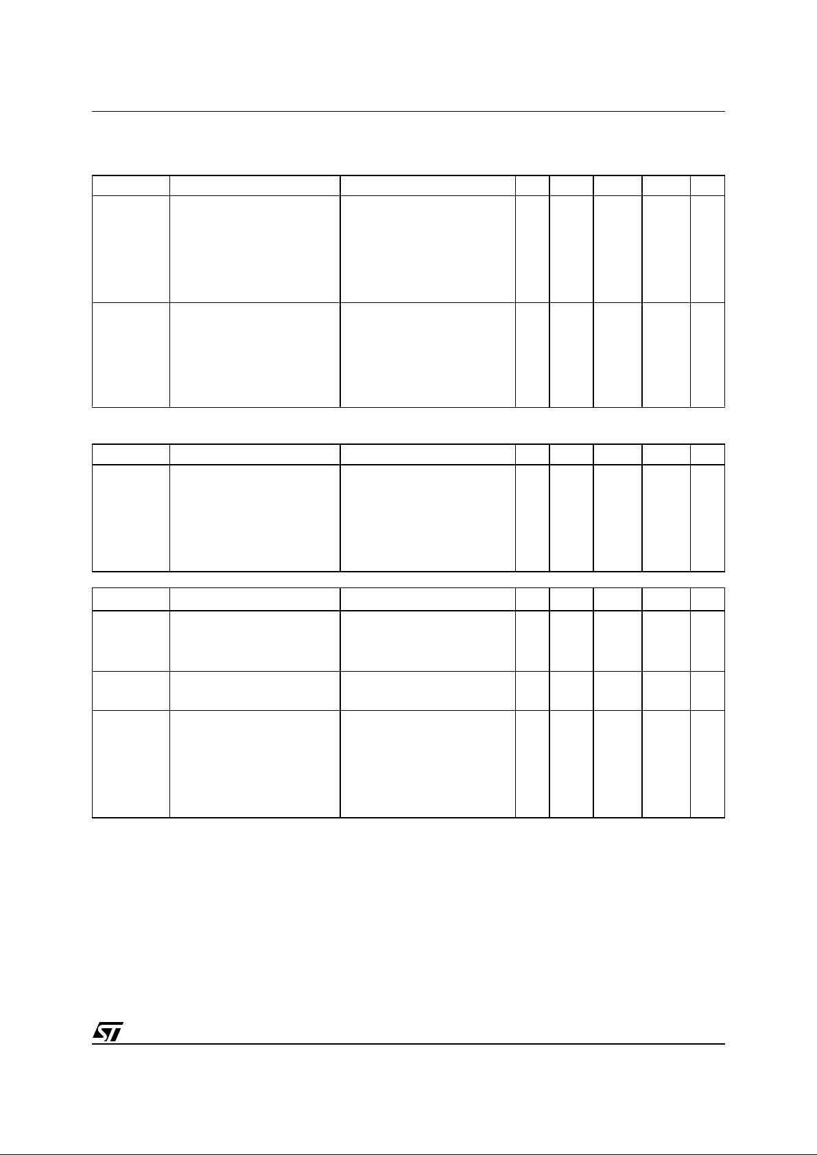
ELECTRICAL CHARACTERISTICS (continued)
SWITCHING ON
Symbol Parameter Test Conditions Min. Typ. Max. Unit
N-CHANNEL
= 15 V ID = 1.75 A
V
t
d(on)
Turn-on Delay Time
R
DD
G
= 4.7
Ω
VGS = 4.5 V
P-CHANNEL
t
r
Rise Time
V
= 15 V ID = 1.5 A
DD
R
G
= 4.7
Ω
VGS = 4.5 V
(Resistive Load, Figure 1)
N-CHANNEL
Qg
Q
Q
Total Gate Charge
gs
gd
Gate-Source Charge
Gate-Drain Charge
VDD=24V ID=3.5A
=4.5V
V
GS
P-CHANNEL
V
= 24V ID = 3A VGS = 4.5V
DD
(see test circuit, Figure 2)
SWITCHING OFF
Symbol Parameter Test Conditions Min. Typ. Max. Unit
N-CHANNEL
= 15 V ID = 1.75 A
V
t
d(off)
Turn-off Delay Time
R
DD
G
= 4.7
Ω
VGS = 4.5 V
P-CHANNEL
t
f
Fall Time
V
= 15 V ID = 1.5 A
DD
R
G
= 4.7
Ω
VGS = 4.5 V
(Resistive Load, Figure 1)
SOURCE DRAIN DIODE
Symbol Parameter Test Conditions Min. Typ. Max. Unit
n-ch
p-ch
n-ch
p-ch
n-ch
p-ch
n-ch
p-ch
n-ch
p-ch
n-ch
p-ch
n-ch
p-ch
27
14.5
40
37
8.5
4.8
2
1.7
4
2
30
90
20
23
12
7
ns
ns
ns
ns
nC
nC
nC
nC
nC
nC
ns
ns
ns
ns
I
SD
I
SDM
V
SD
t
rr
Q
rr
I
RRM
(
Pulsed: P ul se duration = 300 µs, duty cycle 1.5 %.
∗)
(
Pulse widt h l i m i ted by safe operating area.
•)
Source-drain Current
(
•)
Source-drain Current (pulsed)
(
∗)
Forward On Voltage
Reverse Recovery Time
Reverse Recovery Charge
Reverse Recovery Current
I
= 3.5 A VGS = 0
SD
I
= 3 A VGS = 0
SD
N-CHANNEL
ISD = 3.5 A di/dt = 100A/µs
=15 VTj =150 oC
V
DD
P-CHANNEL
= 3 A di/dt = 100A/µs
I
SD
=15 VTj =150 oC
V
DD
(see test circuit, Figure 3)
n-ch
p-ch
n-ch
p-ch
n-ch
p-ch
n-ch
p-ch
n-ch
p-ch
n-ch
p-ch
28
35
18
25
1.3
1.5
3.5
3
14
12
1.2
1.2
A
A
A
A
V
V
ns
ns
nC
nC
A
A
3/10

STS3C3F30L
Safe Operating Area n-ch Thermal Impedance n-ch
Output Characteristics n-ch Transfer Characteristics n-ch
Transconductan ce n- ch Static Drain-source On Resistance n-ch
4/10

STS3C3F30L
Gate Charge vs Gate-source Voltage n-ch Capacitance Variations n-ch
Normalized Gate Threshold Voltage vs Temperature n-ch Normalized on Resistance vs Temperature n-ch
Source-drain Diode Forward Characteristics n-ch
5/10

STS3C3F30L
Safe Operating Area p-ch Thermal Impedance p-ch
Output Characteristics p-ch Transfer Characteristics p-ch
Transconduc tance p-ch Static Drain-source On Resistance p-ch
6/10

STS3C3F30L
Gate Charge vs Gate-source Voltage p-ch Capacitance Variations p-ch
Normalized Gate Threshold Voltage vs Temperature p-ch Normalized on Resistance vs Temperature p-ch
Source-drain Diode Forward Characteristics p-ch
7/10

STS3C3F30L
Fig. 1: Switching Times Test Circuits For Resistive
Load
Fig. 3: Test Circuit For Diode Recovery Behaviour
Fig. 2: Gate Charge test Circuit
8/10

SO-8 MECHANICAL DATA
STS3C3F30L
DIM.
MIN. TYP. MAX. MIN. TYP. MAX.
A1.750.068
a1 0.1 0.25 0.003 0.009
a2 1.65 0.064
a3 0.65 0.85 0.025 0.033
b 0.35 0.48 0.013 0.018
b1 0.19 0.25 0.007 0.010
C 0.25 0.5 0.010 0.019
c1 45 (typ.)
D 4.8 5.0 0.188 0.196
E 5.8 6.2 0.228 0.244
e1.27 0.050
e3 3.81 0.150
F 3.8 4.0 0.14 0.157
L 0.4 1.27 0.015 0.050
M0.60.023
S 8 (max.)
mm inch
0016023
9/10

STS3C3F30L
Information furnished is believed to be accurate and reliable. However, STMicroelectronics assumes no responsibility for the consequences
of use of such information nor for any infringement of patents or other rights of third parties which may result from its use. No license is granted
by implic ation or oth erwise under any patent or pat ent rights of STMicroelectronic s. Specifications mentioned in this publication are subject
to change without notice. This publication supersedes and replaces all information previously supplied. STMicroelectronics products are not
authorized for use as critical comp onents in life support devi ces or systems wi thout express written approval of STM i croelectronics.
The ST logo is registered trademark of STMicroelectronics
2002 STMi croelectr oni cs - All Righ ts Reserved
All other na m es are the prop erty of their res pective ow ners.
Australi a - Brazil - Canada - China - F i nl and - France - Germany - H ong Kong - India - Israel - Italy - Japan - Mal aysia - Malta - Morocco -
Singap ore - Spain - Sweden - Switzerland - Uni ted Kingdom - United States.
STMicroelectronics GROUP OF COMPANIES
http:// www.st.com
10/10
 Loading...