

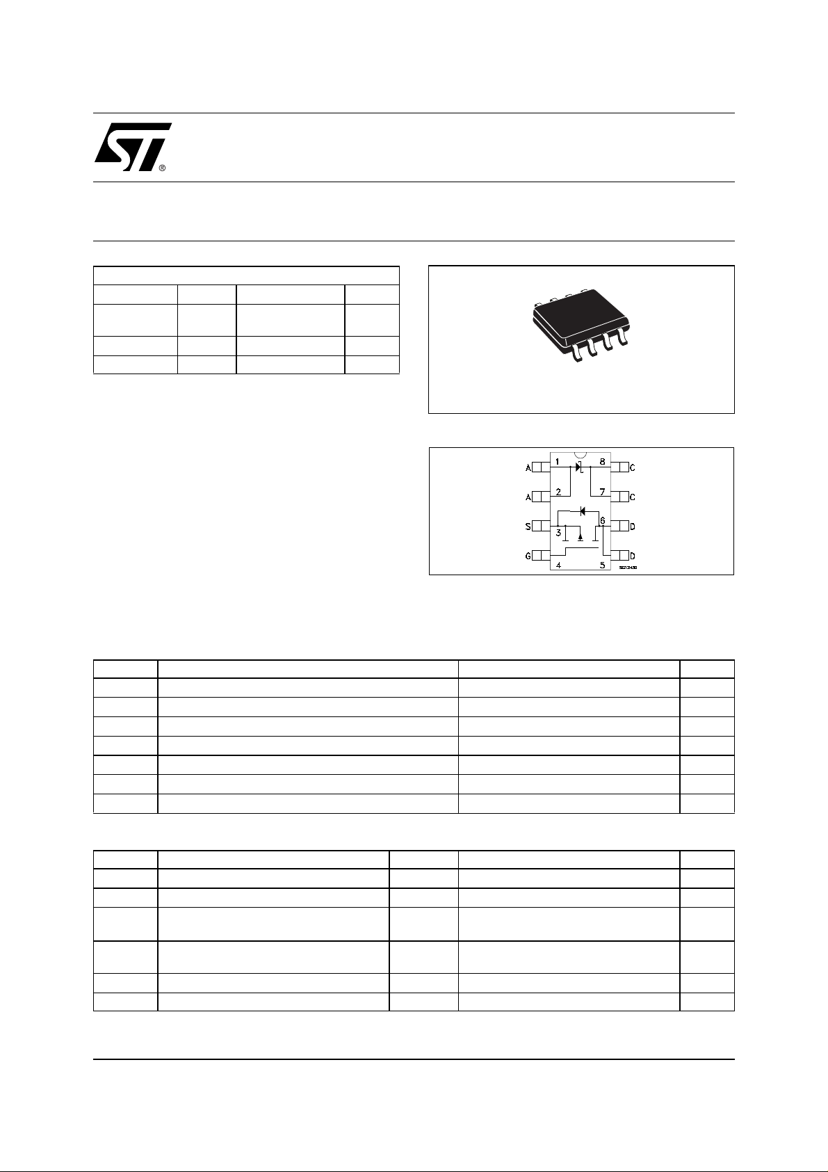
STS2DPFS20V
P-CHANNEL 20V - 0.14 Ω - 2.5A SO-8
2.7V-DRIVE STripFET™ II MOSFET PLUS SCHOTTKY DIODE
MAIN PRODUCT CHARACTERISTICS
MOSFET
SCHOTTKY
V
DSS
20 V
I
F(AV)
3 A 30 V 0.51 V
R
DS(on)
< 0.20Ω (@4.5V)
< 0.25Ω (@2.7V)
V
RRM
DESCRIPTION
This product associates the latest low voltage
StripFETœ in p-channel version to a low drop
Schottky diode. Such configuration is extremely
versatile in implementing, a large variety of DC-DC
converters for printers, portable equipment, and
cellular phones.
2.5 A
V
F(MAX)
I
D
SO-8
INTERNAL SCHEMATIC DIAGRAM
MOSFET ABSOLUTE MAXIMUM RATINGS
Symbol Parameter Value Unit
I
V
DM
V
DGR
V
I
I
P
Dain-source Voltage (VGS = 0)
DS
Drain-gate Voltage (RGS = 20 kW)
Gate- source Voltage ± 12 V
GS
Drain Current (continuous) at TC = 25°C
D
Drain Current (continuous) at TC = 100°C
D
(•)
Drain Current (pulsed) 10 A
Total Dissipation at TC = 25°C
tot
20 V
20 V
2.5 A
1.58 A
2W
SCHOTTKY ABSOLUTE MAXIMUM RATINGS
Symbol Parameter Value Unit
V
RRM
I
F(RMS)
I
F(AV)
I
FSM
I
RSM
dv/dt Critical Rate Of Rise Of Reverse Voltage 10000 V/µs
(•) Pulse width limited by safe operating area
Note: For the P-CHANNEL MOSFET actual polarity of voltages and current has to be reversed
.
Repetitive Peak Reverse Voltage 30 V
RMS Forward Curren 20 A
=125 oC
T
Average Forward Current
Surge Non Repetitive Forward Current
Non Repetitive Peak Reverse Current tp=100 µs1 A
L
δ =0.5
tp= 10 ms
Sinusoidal
3A
75 A
1/8November 2002
STS2DPFS20V
TERMAL DATA
Rthj-amb
Rthj-amb
T
stg
T
(*)
When M ounted on 1 in ch
(*)
Thermal Resistance Junction-ambient MOSFET
(*)
Thermal Resistance Junction-ambient SCHOTTKY
Storage Temperature Range
Maximum Lead Temperature For Soldering Purpose
j
2
FR-4 board, 2 oz of Cu and t [ 10 sec
MAX
62.5
100
-55 to 150
150
o
C/W
o
C/W
o
C
o
C
ELECTRICAL CHARACTERISTICS (T
= 25 °C unless otherwise specified)
case
OFF
Symbol Parameter Test Conditions Min. Typ. Max. Unit
= 250 µA, VGS = 0
I
D
= Max Rating
V
DS
V
= Max Rating TC = 125°C
DS
V
= ± 12 V
GS
20 V
1
10
±100 nA
ON
V
(BR)DSS
I
DSS
I
GSS
(1)
Drain-source
Breakdown Voltage
Zero Gate Voltage
Drain Current (V
GS
Gate-body Leakage
Current (V
DS
= 0)
= 0)
Symbol Parameter Test Conditions Min. Typ. Max. Unit
V
GS(th)
R
DS(on)
Gate Threshold Voltage
Static Drain-source On
Resistance
V
= VGS ID = 250 µA
DS
= 4.5 V ID = 1 A
V
GS
VGS = 2.7 V ID = 1 A
0.6 V
0.14
0.20
0.20
0.25
SCHOTTCKY STATIC ELECTRICAL CHARACTERISTICS
Symbol Parameter Test Conditions Min. Typ. Max. Unit
T
= 25 oC VR= 30 V
(*)
I
R
(*)
V
F
Reversed Leakage Curren t
Forward Voltage drop
J
= 125 oC VR= 30 V
T
J
T
= 25 oC IF= 3 A
J
= 125 oC IF= 3 A
T
J
30
0.40
0.2
100
0.51
0.46
µA
µA
Ω
Ω
mA
mA
mA
mA
DYNAMIC
Symbol Parameter Test Conditions Min. Typ. Max. Unit
(*)
g
fs
C
iss
C
oss
C
rss
2/8
Forward Transconductance
Input Capacitance
Output Capacitance
Reverse Transfer
Capacitance
V
= 15 V ID=1 A
DS
= 15V, f = 1 MHz, VGS = 0
V
DS
4S
315
87
17
pF
pF
pF
STS2DPFS20V
ELECTRICAL CHARACTERISTICS (continued)
SWITCHING ON
Symbol Parameter Test Conditions Min. Typ. Max. Unit
= 10 V ID = 1 A
t
d(on)
t
Turn-on Delay Time
r
Rise Time
V
DD
RG= 4.7 Ω VGS = 4.5 V
(Resistive Load, Figure 3)
Q
g
Q
gs
Q
gd
Total Gate Charge
Gate-Source Charge
Gate-Drain Charge
= 10V ID= 2A VGS=4.5V
V
DD
SWITCHING OFF
Symbol Parameter Test Conditions Min. Typ. Max. Unit
= 10 V ID = 1 A
t
d(off)
t
Turn-off Delay Time
f
Fall Time
V
DD
RG= 4.7Ω, V
GS
= 4.5 V
(Resistive Load, Figure 3)
SOURCE DRAIN DIODE
Symbol Parameter Test Conditions Min. Typ. Max. Unit
I
SD
I
SDM
V
SD
t
rr
Q
rr
I
RRM
(*)
Pulsed: P ul se duration = 300 µs, duty cycle 1.5 %.
(
•)Pulse width limited by s afe operating area.
Source-drain Current
)
Source-drain Current (pulsed)
(•
(*)
Forward On Voltage
Reverse Recovery Time
Reverse Recovery Charge
Reverse Recovery Current
I
= 2 A VGS = 0
SD
= 2 A di/dt = 100A/µs
I
SD
V
= 10 V Tj = 150°C
DD
(see test circuit, Figure 5)
38
30
3.5
0.34
0.8
45
11
15
7.5
1
4.7 nC
2
10
1.2 V
ns
ns
nC
nC
ns
ns
A
A
ns
nC
A
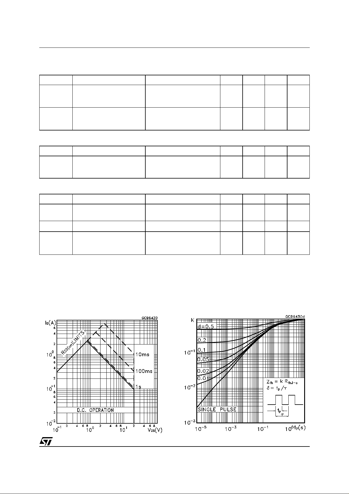
Safe Operating Area
Thermal Impedance
3/8

STS2DPFS20V
Output Characteristics Transfer Characteristics
Transconductance Static Drain-source On Resistance
Gate Charge vs Gate-source Voltage Capacitance Variations
4/8

STS2DPFS20V
Normalized Gate Threshold Voltage vs Temperature Normalized on Resistance vs Temperature
Source-drain Diode Forward Characteristics Normalized Breakdown Voltage vs Temperature.
. .
5/8

STS2DPFS20V
Fig. 1: Unclamped Inductive Load Test CircuitFig. 1: Unclamped Inductive Load Test Circuit Fig. 2: Unclamped Inductive Waveform
Fig. 3: Switching Times Test Circuits For Resistive
Load
Fig. 5: Test Circuit For Inductive Load Switching
And Diode Recovery Times
Fig. 4: Gate Charge test Circuit
6/8

SO-8 MECHANICAL DATA
STS2DPFS20V
DIM.
MIN. TYP. MAX. MIN. TYP. MAX.
A1.750.068
a1 0.1 0.25 0.003 0.009
a2 1.65 0.064
a3 0.65 0.85 0.025 0.033
b 0.35 0.48 0.013 0.018
b1 0.19 0.25 0.007 0.010
C 0.25 0.5 0.010 0.019
c1 45 (typ.)
D 4.8 5.0 0.188 0.196
E 5.8 6.2 0.228 0.244
e1.27 0.050
e3 3.81 0.150
F 3.8 4.0 0.14 0.157
L 0.4 1.27 0.015 0.050
M0.60.023
S 8 (max.)
mm inch
0016023
7/8

STS2DPFS20V
Information furnished is believed to be accurate and reliable. However, STMicroelectronics assumes no responsibility for the con sequences
of use of such information nor for any infringement of patents or other rights of third parties which may result from its use. No license is granted
by implic ation or o therwise under any patent or patent rights of STMicroelectron i cs. Speci fications mentioned i n this publication are subject
to change without notice. This publication supersedes and replaces all information previously supplied. STMicroelectronics products are not
authorized for use as c ri t i cal components in life support dev i ces or systems wi thout exp ress written approval of STMicroel ectronics.
The ST log o i s registered tradema rk of STMicroelectronics
2002 STMicroelectronic s - All Right s Reserved
All other names are the property of their resp ective owners.
Australi a - Brazil - Canada - Chin a - F i nl and - Franc e - Germany - Hong Kong - India - Israel - Italy - Japan - Malays i a - M al ta - Morocco -
Singapor e - S pai n - Sweden - S witzerland - United Kingdom - Unit ed States.
STMicroelectron ics GROUP OF COMPANIES
http://www.st.com
8/8
 Loading...